Industry News
The latest news on the semiconductor and electronic-parts industry .
RISC-V Summit Europe 2026: Industry and Academia Unite in Bologna to Advance Open Hardware
RISC-V Summit Europe is coming to Bologna, Italy, with a program that reflects just how far the ecosystem has come since we gathered in Paris a year ago. Taking place June 8–12 2026 at the Palazzo dei Congressi, the summit unites members, manufacturers, researchers, public institutions, academics and students, all helping to nurture the RISC-V open standard instruction set architecture (ISA). There is something very fitting about the RISC-V ecosystem gathering in Bologna. The city’s university, the oldest in the Western world, was founded in 1088 by students who wanted to take their education into their own hands. Over 900 years later, that same instinct surfaced at University of California Berkeley, where students and staff created RISC-V in 2010: an ISA deliberately designed to put the ability to learn and build silicon chips into anyone’s hands. Yet Bologna is no incidental host. The University of Bologna (‘Unibo’) has been at the heart of European RISC-V research for over a decade, through the long-running PULP RISC-V research platform. It’s also a key partner in TRISTAN, the EU Chips Joint Undertaking-funded initiative to expand and industrialize the European RISC-V ecosystem. An engaging schedule of speaker sessions and workshops The core summit runs from Tuesday, June 9 to Thursday, June 11, with Monday activities focused on our Intro to RISC-V and new developer workshops, as well as working group meetings. Plenary sessions begin on Tuesday morning at 9am. The conference program will help attendees explore both commercial and research applications of RISC-V, with sessions spanning embedded systems, AI, automotive, high-performance computing, security, space, software enablement and open hardware research. In particular, the recent arrival of silicon compliant with the RVA23 hardware profile will undoubtedly shape many of this year’s keynotes, demos and show floor conversations. While the number of exciting sessions is far too many to detail here, some of our expected highlights include: Open-Source Microprocessors in the Internet of Trees One of our favorite use cases of edge ML in recent years saw devices deployed throughout the rainforest to listen to the sound of chainsaws, denoting illegal logging activity. This session explores how RISC-V is now being used to take this ‘Internet of Trees’ concept further; deploying ultra-low-power, secure, and custom processors throughout forests to turn them into intelligent, real-time sensing networks for monitoring biodiversity, climate, and environmental change. It’ll be delivered by Marcello Zuffo and Laisa-USP Caroline Costa de Biase of the University of São Paulo. RISC-V for Low-Power AI in Next-Generation Smart Glasses Marco Fariselli of Italian eyewear corporation Luxottica will examine one of the toughest engineering balancing acts in consumer hardware: delivering advanced AI features in smart glasses without reducing battery life or wearability. We look forward to hearing how RISC-V’s adaptability is finally opening the door for product-driven companies to build highly specialized silicon that’s light enough that the wearer forgets it’s there. RISC-V: Enabling Open Physical AI Luca Benini is Professor at the University of Bologna, Chair of Digital Circuits and Systems at ETH Zurich, and leads PULP. He’ll be delivering a keynote on Enabling Open Physical AI (being AI systems that perceive, reason about, and interact with the real world, rather than existing solely in software). Benini promises concrete examples of how RISC-V enables deep domain specialization for energy efficient, safe and robust Physical AI systems, from robots to cars to satellites. Matrix Extensions for RISC-V: Delivering on the Promise Matrix multiplication is fundamental to many AI workloads, and work has been ongoing for several years now to define how to standardize matrix compute capability within the RISC-V architecture. At Summit Europe in Paris last year, this effort was restructured into multiple complementary approaches, in recognition that the breadth of the RISC-V ecosystem requires a family of solutions rather than one rigid standard. In Bologna, VRULL GmbH’s Philipp Tomsich will deliver the first significant report on progress across the matrix extension family, as two of the extensions – the Integrated Matrix Extension (IME) and the Vector Matrix Extension (VME) – converge on specification freeze, with compiler unification work underway to give AI frameworks a single path covering both. A great opportunity to get up to speed on matrix just before it lands. Beyond Privilege: The RISC‑V Isolation Toolbox from Microcontrollers to Confidential Computing The philosophy of complementary approaches rather than a single rigid standard isn’t unique to matrix extensions: it runs just as deeply through RISC-V’s approach to security. Rather than treating isolation as a mechanism bolted on at the end, the community has built a layered toolbox of complementary techniques that can be combined differently depending on the threat model and the hardware. Andrew Dellow of Qualcomm will walk us through that toolbox in Bologna: from physical memory protection in microcontrollers, through virtualization and hardware-enforced compartmentalization, up to Supervisor Domains – an emerging architectural direction that pushes isolation further still. A session of enormous relevance that belongs on every attendee’s list. On the show floor, attendees will discover the latest technical demonstrations from RISC-V members, while our Developer Zone showcases a selection of RISC-V hardware, from $5 embedded boards to AI powerhouses and complex FPGA devices. You’ll also find posters, academic demos, developer workshops, technical working group meetings and thematic sessions, including RISC-V in Space and TRISTAN. Empowered by our sponsors RISC-V Summit Europe 2026 is organized by RISC-V International, the University of Bologna and Planning. Platinum sponsors include BOSC, E4 Computing, Next Silicon, Nuclei Systems and MIPS. Gold sponsors include Breker Systems, CEA, Epic Semi, ESWIN Computing, SiFive, Tenstorrent, Tristan+Isolde and XUANTIE. Silver sponsors include Akeana, Andes, Arteris, Baya Systems, Barcelona Supercomputing Center, Chips-IT, CircuitSutra, GLIWA, Lauterbach, Microchip Technology, OmniTrust, PlanV, Pulp Platform, Real Intent, RISE, SEGGER, SpacemiT and Tera Pines. Online registration is open until Friday, June 5th, with on-site registration available at the Summit venue after that date. Registration includes access to the core summit from Tuesday, June 9 to Thursday, June 11, including plenaries, poster sessions, demo theater, the evening events and the exhibition area. _The RISC-V Summit is a community-curated content, research and innovation driving the next wave of growth for RISC-V._ 0 comments

Inside Europe’s Chip Rethink: Why Fabs Weren’t Enough and Why Spain Matters
Europe’s semiconductor strategy is undergoing a quiet but significant reversal. After years of focusing on manufacturing capacity and supply-chain resilience, a new industry blueprint argues that Europe started in the wrong place. The next phase of policy, it says, must focus less on fabs and more on the conditions that create them: chip design, startup scale, local demand, and faster execution. “We have to build the house from the basement, not from the roof,” Maria Marced told EE Times. Chair of the Industry Advisory Group (IAG) and past president of TSMC EMEA, Marced said Europe’s first semiconductor push emphasized manufacturing before ensuring enough local technology and market demand existed to support it. That same argument is echoed by Francesc (Cesc) Guim, whose Barcelona-based startup, Openchip, was one of only two fabless AI chip companies in the IAG. “It doesn’t make sense to invest in advanced fabs if you don’t have the demand to fill them,” Guim told EE Times. “Demand creates local companies that do chips. Once you create demand, you incentivize the creation of local manufacturing.” What makes that rethink especially notable is where two of its clearest voices are coming from: Spain. Long overshadowed by semiconductor heavyweights such as Germany, France, and the Netherlands, Spain is emerging as a more influential player in Europe’s next chip debate—through design startups, photonics, quantum technologies, and a growing talent base. In Marced and Guim, it also has two industry figures helping shape the policy response from inside Brussels. Why fabs weren’t enough The IAG emerged after the European Commission sought feedback last fall on the performance of the first European Chips Act. That process sparked a discussion that informs what many in the industry now call Chips Act 2.0. Industry Advisory Group’s Maria Marced According to Marced, the IAG was formed partly because companies felt they were not being heard directly enough. “Industry in general was complaining that once again the EU was asking for advice from other parties, but not from industry itself,” she said. “Associations are important, member states are important, but companies also wanted to be heard directly.” The Commission responded by assembling a 16-company group spanning the value chain: equipment makers, foundries, integrated device manufacturers, fabless startups, and end users in sectors such as telecom, defense, and automotive. The mandate was not just to submit comments but to produce a common blueprint. Guim said that diversity made the process very different from a normal consultation. “You pick companies that represent different realities of the European landscape,” he said. “Then you try to get them to provide a unified input. That is much harder than everyone sending separate opinions.” Marced acknowledged the internal tensions. “It was not easy at all,” she said. “You can imagine the tension between the IDMs and the fabless, between mature-node priorities and leading-edge priorities. We needed a lot of diplomacy.” But what resulted was a March 2026 report calling for a broader industrial policy centered on demand, resilience, and improved framework conditions. The first Chips Act was shaped by the global shortages of 2020–2023, when Europe’s immediate concern was to bring more manufacturing capacity onto EU soil. The IAG report credits Chips Act 1.0 with raising political awareness, enabling state aid flexibility, and supporting fab investments. But it also says the strategy was too narrow. Despite billions in support, Europe continued to lose market share in a semiconductor market that was expanding faster elsewhere. The IAG argues that focusing on manufacturing alone ignored key parts of the value chain, especially design, product development, and demand generation. “The first thing you have to do is incentivize design by helping design companies, especially fabless companies, to design chips,” Marced said. “If we don’t help those startups to prototype, to tape out, to reach customers, it will be impossible to have local content and therefore local demand for local chips.” “If nobody is buying the chips, the fab is not sustainable,” Guim said. “A fab needs customers, volume, and long-term visibility. Demand is not a side issue; it is the foundation.” Maria Marced symbolically handing over the report to Henna Maria Virkkunen, EVP of the European Commission for Technological Sovereignty, Security and Democracy. Creating demand and injecting capital If subsidizing factories is politically visible, creating demand is much harder. It means aligning procurement policy, encouraging end-user industries to work with European chip suppliers, backing new design firms, and sometimes favoring local technologies over established global incumbents. The IAG report calls for pre-commercial commitments, advanced purchase commitments, and strategic public procurement programs in critical sectors. It also proposes a “Trusted Supplier of Chips” concept tied to resilience and economic security. According to Marced, industrial players pressed for stronger action, including measures that would give European technologies greater opportunity in public-sector projects. “The European industry needs and wants this,” she said. Openchip’s Francesc (Cesc) Guim “If Europe does not get into 20% to 30% of consuming local technology, I would say the goal is not going to be achieved,” Guim said. “You need reference customers. You need scale. Otherwise, startups stay small, and customers keep buying elsewhere.” That illustrates the central tension facing Chips Act 2.0: Industry wants stronger demand-side tools, while Brussels must weigh competition rules, trade concerns, and political sensitivities. Demand is only part of the challenge; the second is money. Asked to name the biggest structural barrier facing semiconductor startups in Europe, Guim answered in one word: “Capital.” He contrasted Europe with the U.S., where investors are often more willing to back long-horizon chip bets. “Here, we want to play Champions League,” he said. “But it’s impossible if people expect quick returns from businesses that need years of development.” The IAG report proposes a dedicated blended finance facility offering €30 million to €500 million per company for semiconductor scale-ups, plus a separate €20 billion to €30 billion startup and scale-up fund. Marced said financing must be matched by speed. “It’s too bureaucratic, it’s too lengthy, it’s too cumbersome,” she said of current approval and funding processes. “Semiconductors move fast. If Europe takes too long, the opportunity moves somewhere else.” That concern runs throughout the report, which calls for six-month approval timelines, simplified state aid procedures, and even automatic approvals if deadlines are missed. Why Spain now matters Spain is not Europe’s largest semiconductor base. But it increasingly represents the kind of distributed innovation model that Europe may need more of. Marced pointed to photonics clusters in Barcelona, Valencia, Malaga, and Vigo, alongside strong universities and growing technical talent. “The area where Spain is quite relevant today is photonics,” she said. “And we have talent. We have very good universities. The challenge is converting that talent into growth and success.” Guim sees a broader ecosystem forming around AI chips, quantum technologies, research institutes, and the Barcelona Supercomputing Center. “We have the talent, and we have the people,” he said. “What talent needs is vision, challenge, and some level of security.” That message resonates beyond Spain. Europe’s future semiconductor growth may come not only from established hubs but from newer clusters able to combine research, entrepreneurship, and specialized talent. If the IAG process demonstrates anything, it is that Europe’s semiconductor industry is more aligned than it has been in years. Large incumbents and startups may differ on priorities, but they broadly agree on three needs: more demand, more scale, and faster execution. The March report gives Brussels a roadmap grounded in industry realities. Whether Chips Act 2.0 can turn that roadmap into policy—and policy into results—remains the unanswered question. Europe now appears to understand that fabs alone will not secure its semiconductor future. The harder test is whether it can build the foundation quickly enough.

Antenna-First Design: The RF Shift IoT Cannot Avoid
I have seen this pattern more times than I care to count. A team completes every schematic review without a red flag, selects a certified module, and confirms the antenna fits within the allotted footprint. Then the first prototype comes back from the chamber with weak radiated power—or worse, a certification result that sends the whole program back for another spin. In every one of those cases, the root cause was not the component. It was the RF system built around it—designed without ever treating the antenna as an integrated part of that system from day one.That is an engineering process failure, and it is one we can fix. The Antenna-Last Habit Is Costing Us Spins The default sequence on most wireless product programs goes like this: define the application, select the module, shape the enclosure, route the PCB, then find an antenna that fits whatever space is left. When board area is generous and RF requirements are straightforward, you can get away with it. We no longer have that luxury. Today’s wireless devices are shrinking while simultaneously adding bands and tightening certification requirements. Berg Insight estimates that annual cellular IoT antenna shipments hit 757 million units in 2025—with 90% of them internal. Every one of those antennas must radiate from inside a product where the PCB ground plane, enclosure, battery, and surrounding metalwork become active participants in the radiating structure. That constraint has an uncomfortable implication: changing any one of those structural elements after antenna position is set can shift impedance, resonant frequency, or radiation pattern enough to invalidate the design. At sub-GHz and low cellular bands, the margin shrinks further—wavelength is inversely proportional to frequency, so these antennas need more electrical length and more help from the host structure. A ground plane that is too small or broken by slots does not just degrade performance—it can make a design that tuned cleanly on the bench fail completely in the final product. When teams discover this late, the consequences compound. We reach for a matching network to correct frequency shifts. TRP shortfalls found at certification force layout or enclosure changes that reset tooling. Each fix restarts a timeline that was already committed. The further downstream we find this, the fewer options we have. Datasheets Do not Predict Product Performance—Integration Does I want to address a misconception that creates false confidence early in a program. Antenna datasheets describe behavior on a reference board with controlled clearance and defined measurement conditions. That reference board is engineered to show the antenna at its best:clean ground plane, proper keep-out, no enclosure effects, no battery pressing against the element. A finished wireless product presents a fundamentally different RF environment. A tracker bolted to a metal asset changes the ground plane geometry. A meter mounted inside a metal cabinet creates reflections and blockage. A wearable pressed against skin introduces lossy tissue into the near field. Each deployment shifts the impedance the antenna sees and the radiation the device produces. The variables that determine the outcome are well understood by anyone who has done this work: antenna position relative to metal and ground, whether the keep-out zone is actually clear of copper, components and mechanical parts, whether the feedline is properly referenced to 50Ω across its full length, and whether the matching network compensates for the real-device environment rather than masking a deeper layout problem. These are not antenna selection problems.They are integration decisions made—or not made—during PCB layout. One clarification worth stating explicitly for our teams: bench return-loss measurements and OTA measurements answer different questions. Bench measurement tells you whether the antenna is matched. OTA measurement—TRP for radiated power, TIS for receive sensitivity—tells you whether the complete device actually works in the real world. Both are necessary. Neither replaces the other. Multi-Radio Designs Multiply the Integration Risk The integration gap widens significantly when multiple radios share a small enclosure, and that is the reality of most modern IoT designs. A typical wireless tracker might combine LTE-M with GNSS and Bluetooth. A smart meter might run cellular alongside a short-range wireless stack. Each radio brings its own bands, power levels, sensitivity requirements, and antenna constraints. The coexistence problem is quantifiable,and it is severe. A cellular transmitter operates around 23 dBm. A GNSS receiver is trying to detect signals around −130 dBm.That is a 150+ dB difference. If cellular energy couples into the GNSS receive path, the receiver desensitizes—resulting in slow positioning, unstable fix, or complete failure. Antenna spacing, filtering, grounding, and shielding can address this. But they must be considered during layout. By the time coexistence problems show up in the chamber, every layout decision that could have prevented them is already locked. Every radio added to a design is another constraint our layout engineers need to understand from the start of the project—not as an afterthought during bring-up. Certification Tests the System—Not Just the Antenna There is a persistent misconception I have heard from program managers and even some engineers: that we are“certifying the antenna.”We are not. For wireless products, the device is certified. The antenna is one component of the RF system under test. Two OTA measurements decide the outcome: TRP, which captures how effectively the device radiates power, and TIS, which captures how well it receives weak signals. Both are shaped by antenna placement, board layout, noise floor, and enclosure effects. Both reflect integration quality—not component quality alone. A device can show clean return loss on the bench and still fail TRP in the chamber because radiation is absorbed, blocked, or redirected by the enclosure and internal structures. The bench measurement tells you the antenna is matched. The chamber tells you whether the complete device radiates or receives efficiently. The commercial consequences of discovering an RF integration problem at certification are significant. As Berg Insight notes, cellular device certification spans regulatory, industry, operator, and application-specific requirements. By the time a device is in the certification chamber, enclosure tooling is paid for,component sourcing is committed, operator approval timelines are running, and launch dates are on the record with customers. A board respin at that point is not just an engineering cost.It is a product launch delay.That is not a risk any of us should be accepting when it is preventable. What Antenna-First Engineering Actually Means in Practice Antenna-first design does not mean selecting an antenna before selecting a radio. It means treating antenna integration as a layout requirement from the start—not a post-layout correction. Concretely, this means our teams evaluate whether antenna position, board dimensions, and ground plane will support the required bands before the first layout is locked. A structured approach toIoT antenna designstarts with these constraints. We review clearance zones against actual component placement. We review clearance zones against actual component placement. We verify that the feed transmission line preserves 50Ω impedance. We confirm the matching network is accessible for tuning when the first prototype arrives. These are not heroic engineering acts. They are process disciplines that prevent expensive late discoveries. The goal is not to eliminate RF measurement—RF still requires measurement, full stop. The goal is to make the first prototype close enough to expected behavior that measurement confirms the design rather than reveals its problems. When that happens, the lab becomes a validation step. When it does not, the lab becomes a discovery phase that feeds an unplanned respin cycle. Managing RF Risk with the Right Tools and Partners One approach worth understanding is Ignion’s Virtual Antenna® technology—a three-part architecture comprising an antenna booster, a tunable matching network, and the PCB ground plane, with over 100 million devices deployed. What makes this model relevant to our process discussion is the matching network path: it gives engineering teams a tuning mechanism accessible during DVT without requiring a board respin. Their Oxion™ platform enables pre-prototype evaluation of placement, clearance, and ground plane constraints against actual layout—exactly the kind of upstream validation our teams need to be doing regardless of which antenna solution they choose. When a prototype shows a frequency shift due to enclosure effects or component proximity, having a matching network that can compensate—provided the underlying layout supports it—is operationally meaningful. The broader point: tools and partners that support pre-prototype RF evaluation and DVT-stage tuning are worth integrating into our standard development workflow. The alternative—treating RF as something we validate at the end—has a well-documented cost in respins, delays, and certification failures. The Direction of Travel Is Clear Berg Insight projects cellular IoT antenna shipments will exceed one billion units annually by 2030. More internal antennas, more compact enclosures, more bands per product, more certification paths per region. The integration challenge is not getting simpler. The teams that manage this well in the years ahead will not differentiate by picking better antennas.They will differentiate by building RF constraints into their process early enough that those constraints shape the design rather than break it. That is the shift I am asking product development engineering teams to make—treat RF integration as a first-class design constraint from day one, not a problem to solve after the layout is locked. Teams that commit to this discipline will spend less time in debug, less time firefighting at certification, and more time moving confidently from DVT through PVT and into a clean product launch. The antenna does not get easier to integrate as the schedule compresses. But the path to launch gets significantly shorter when the hard RF decisions are made at the start of the program, not at the end of it.

Connectivity Revolution or Evolution Inside Data Centers?
AI is radically changing the role of connectivity inside data centers, to the point where intra-data center networks are becoming as critical as the compute itself. The intra-data center backend network (which connects AI accelerators to each other and to memory for workload distribution) is effectively becoming an extension of the computing system. So, are we facing a revolution or an evolution in intra-data center networking? Maybe a mix of both. The revolutionary surge in AI workloads is pushing for new technologies, but these technologies leverage existing approaches, building on a continuum of innovations stretching back years. For decades, copper cables were the default for intra-data center connections. Copper is inexpensive, easy to work with, and effective over short distances. But copper struggles as data rates climb and distances grow, with signal integrity degrading due to attenuation and electromagnetic interference. Optical fiber, on the other hand, can carry far higher data rates over longer distances with minimal signal loss and no electromagnetic effects. Currently, almost all 400 Gbps data center connections beyond approximately 5 m (i.e., any high-performance connection beyond a single rack) have transitioned to optical. Faster AI accelerators are already pushing intra-rack connectivity to switch to optical. Ultimately, every connection inside an AI factory data center will be implemented using optical fibers. The past few years have witnessed an impressive progression of optical link speeds, moving rapidly from 100 Gbps to 400 Gbps to 800 Gbps, and emerging 1.6 Tbps. Meeting the demands of AI training and inference, however, requires more than faster ports. AI redefining data center networks Historically, data centers used a scale-up strategy for growth: a vertical approach that adds bigger servers or more processors to a rack. Modern AI challenges that paradigm. Large AI models and distributed training must orchestrate thousands of processors/accelerators in unison. This means data center buildouts need to scale out, connecting myriads of nodes across racks, rows, and adjacent buildings, to act as one single computing fabric working on shared tasks. While distributed computing isn’t new, the sheer scale and performance of these AI fabrics are unprecedented. Enormous AI training clusters are being built where the scale-out network handling terabits per second of traffic at single-digit microsecond latencies connects thousands of racks each outfitted with dozens of GPUs. Public estimates for large AI clusters suggest (averaging optics across a full fabric) that these deployments can require three to six optical transceivers per GPU. This translates into over a million short‑reach optical transceivers to connect servers to top‑of‑rack leaf switches, and top‑of‑rack leaf switches to spine switches within a single data center with hundreds of thousands of GPUs. In fact, industry analysts such as LightCounting forecast that sales of Ethernet optical transceivers and co-packaged optics will double over the next five years, with intra-data center applications accounting for most of that growth. Global demand is expected to reach hundreds of millions of units annually over the coming years to support a massive deployment of AI clusters. Today’s pluggable optics: FRO, LRO, LPO To support the AI optical explosion, innovation has focused not just on faster links, but on how optical modules themselves are designed and deployed. Inside the data center, power efficiency and density rule. This has resulted in new optical architectures that reduce power consumption and footprint while enhancing deployment flexibility. Traditional pluggable optical modules use fully retimed optics (FRO), which integrate signal processing on both transmit and receive paths. This delivers robust performance and long reach at the expense of power consumption and latency. Newer approaches take a lighter touch. Linear‑receive optics (LRO) simplify the receive path by relying on signal processing in the switch ASIC, significantly reducing module power and latency. Pushing this concept further, linear pluggable optics (LPO, or linear drive) remove active signal processing from the pluggable module altogether, delivering very low power consumption and minimal latency for short‑reach links, provided the host is designed to support this model. Importantly, all three approaches coexist in modern data center networks. FRO continues to serve applications that demand reach and robustness, while LRO and LPO are gaining momentum for high‑volume, short‑reach intra-data center links where efficiency and density are paramount. Together, these approaches illustrate the evolutionary path of optics, balancing performance and power as revolutionary data center networks scale for AI. Tomorrow’s optical evolution: NPO, CPO, XPO Optical pluggables continue to be reimagined. A novel concept called extra-dense pluggable optics (XPO) was introduced by an industry consortium in early 2026 as a way to significantly boost optical front-panel density, a key limiting factor in intra‑data center connectivity. An XPO module delivers an unprecedented 12.8 Tbps of bandwidth, and while it is larger than an octal small form-factor pluggable (OSFP), it still allows for roughly a four-fold increase in front-panel density compared to today’s pluggable solutions. Since XPO integrates liquid cooling, these modules are also capable of supporting more power‑hungry coherent optics. In parallel, the industry has also been exploring more radical optical integration models. At the core of this shift is a simple idea: bringing optics closer to compute or switching reduces signal losses and the power required to compensate for them, while overcoming space limitations in the front-panel. Near‑packaged optics (NPO, also known as on-board optics) move optical engines off the front panel and closer to the switching silicon, reducing electrical distances and improving efficiency. This approach delivers clear gains in power consumption and signal quality but sacrifices flexibility since the optics are no longer easily replaceable. Co‑packaged optics (CPO) take this concept further by integrating optics directly into the switch chip package. By drastically reducing electrical interconnects, CPO promises ultra‑low latency and exceptional energy efficiency. At the same time, it challenges long‑standing assumptions around serviceability, manufacturing, and interoperability. Together, XPO, NPO, and CPO illustrate how the evolution of intra‑data center optics is no longer just about faster links, but about fundamentally re-engineering how optics, electronics, and compute come together in the AI era. Data center connectivity in the AI era is experiencing both a revolution, in terms of requirements and scale, and an evolution, building on decades of optical progress. Read also: At OFC 2026, eXtra-dense pluggable optics (XPO) resonated strongly because it directly addresses the fundamental challenges of next-generation AI infrastructure: bandwidth density, power efficiency, thermal management, and serviceability. RELATED TOPICS:AI ACCELERATOR, AI INFERENCE, CO-PACKAGED OPTICS, DATA CENTERS, EXTRA-DENSE PLUGGABLE OPTICS (XPO), OPTICAL NETWORKS, OPTICS & PHOTONICS COMPANIES:NOKIA _Teresa Monteiro is director of marketing at Nokia, while Rimlee Deb Roy is senior staff market research analyst in Nokia's Optical Product Marketing division._ 0 comments
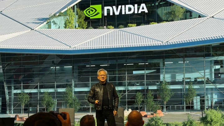
Geopolitics, AI, and Jensen Huang Fuel Electronics’ Rock-and-Roll Era
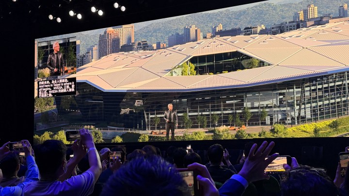
At Computex 2026 this week, the electronics industry hit a clear inflection point: It’s the new rock and roll, proved by a mob of attendees chasing the show’s ultimate star attraction, Nvidia CEO Jensen Huang. Everywhere you turned, whether it was on the show floor at the Tainex halls in Taipei, where the show was held, or at the food night markets, people chased the CEO for selfies, autographs, and just to feel his presence. To many, he’s become a demigod, a rock star, a symbol of the semiconductor industry. It’s like watching the 1964 Beatles movie, “A Hard Day’s Night,” in which fans are constantly chasing the pop group anywhere and everywhere, because they were so hugely popular. Frivolity aside, this tells many stories about where the industry is right now. First, because of the supply chain challenges that Covid-19 brought on in 2020, the general public and politicians became more aware of semiconductors due to chip shortages. Meanwhile, the geopolitical push for chip sovereignty forced the industry into the government agenda and the public spotlight. And finally, there was the ChatGPT moment in November 2022, which triggered the explosion in growth of AI data centers. Fast forward to 2026, and all the electronics industry seems to be talking about is physical AI, humanoid robotics, and agentic AI. In his Monday keynote, Huang unveiled Nvidia’s RTX Spark: a 1-petaflop “superchip” packed with a full CUDA/RTX ecosystem and Windows-native agents. Both Huang from Nvidia and Arm CEO Rene Haas talked about this potentially “reinventing” the Windows PC for “personal AI.” Developed with Microsoft and MediaTek, the massive RTX Spark superchip pairs a Blackwell RTX GPU—featuring 6,144 CUDA cores and fifth-generation, FP4-capable Tensor cores—with a high-performance, 20-core Nvidia Grace CPU via an NVLink-C2C interconnect. Computex and Taiwan thrive on the nation’s pivotal role in the value chain After six years of build-up, the conversation has shifted entirely to GPUs, physical AI, and humanoid robotics—leaving everyone to grapple with AI’s ultimate impact on their lives, future, and livelihoods. And as a result, Computex 2026 brought the crowds in not just for Jensen Huang, but to explore how they can participate in this AI race. The organizers said that the exhibition attracted a total of 111,312 buyers and visitors from 152 countries and regions, including Japan, the U.S., South Korea, China, Hong Kong, Singapore, Vietnam, India, Thailand, and Malaysia. Anchored by Taiwan’s dominant manufacturing ecosystem, the show drew massive crowds by showcasing the entire electronics value chain. This goes far beyond AI chips, IoT, and embedded software. When Taiwan claims “full stack,” it means the literal full stack—from silicon and systems to cables, connectors, enclosures, and consumer gaming PCs. Taiwan is also doing its best to attract startups, with competitions like the IC Taiwan Grand Challenge. One of the eleven winners of this competition, in which startups are given a cash award plus support in connecting with Taiwan’s very useful manufacturing ecosystem and research networks, was a German startup called Linque. The company is focused on delivering AI infrastructure solutions based on programmable silicon photonics technology, with its low-loss photonic fabric optimized for information processing on chip. EE Times spoke to the CEO and co-founder Samarth Vadia. In the video interview, available here, he explains both the company’s proposition and what the award in Taiwan means to the company: You can also listen to the audio-only version below: Audio 3 ### Taiwan’s pivotal role as the epicenter of electronics and AI Two years ago, Jensen Huang said at his keynote at Computex 2024, “The ecosystem here is incredible,” referring to everything from chip manufacturing to packaging, assembly, and test. “This is really an extraordinary place,” he added. Since then, Taiwan’s role has become even more pivotal, and several people are now saying it’s the epicenter of the world’s electronics manufacturing value chain. This week, the Taiwan Stock Exchange announced that its market capitalization had crossed the $5 trillion mark. In its statement, the exchange said, “The milestone reflects the accelerating momentum across Taiwan’s capital markets, which is driven by the AI-led growth spanning semiconductors, hardware, and next-generation applications.” To emphasize this, Brenda Hu, senior VP at the Taiwan Stock Exchange, said, “Today, 90% of AI servers are assembled and manufactured in Taiwan.” And she added, “In 2026 alone, we expect more than 15 AI-related companies to apply for listing on the Taiwan Stock Exchange.”
Manufacturing Accelerates in May Amid Inflation and Geopolitical Headwinds
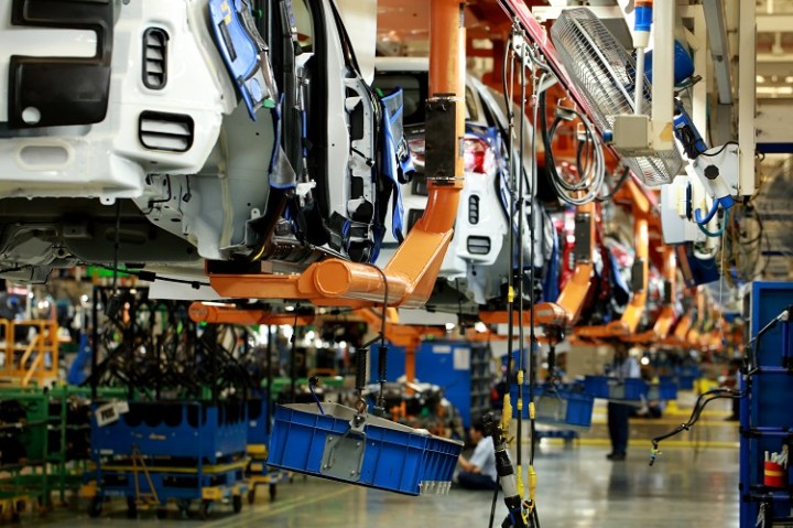
Manufacturing expanded further last month despite Inflation and lower GDP. U.S. manufacturing activity expanded at its fastest pace in two years this May, contrasting with a broader deceleration across the national economy. The Institute for Supply Management reported that its Manufacturing Purchasing Managers’ Index registered 54% in May, up 1.3 percentage points from April. This robust industrial performance diverges from the broader U.S. macroeconomic picture. The U.S. Commerce Department recently revised first-quarter gross domestic product growth down to a 1.6% seasonally and inflation-adjusted annual rate. That downgrade was largely tied to lower estimates for inventory investment and a downward revision in consumer spending on services. Source: Bureau of Economic Analysis Despite this macroeconomic cooling, the industrial sector notched its fifth consecutive month of expansion, reaching its highest level since May 2022. Demand and output strengthen Key manufacturing indicators sent strong positive signals as the second quarter progressed. The New Orders Index expanded for the fifth consecutive month, registering 56.8%, which is up a robust 2.7 percentage points from April. (Source:Institute for Supply Management) Demand sentiment was notably positive, featuring a 1.6-to-1 ratio of positive to negative comments among survey respondents. Output also accelerated, with the Production Index rising to 54.3%, marking a seventh consecutive month of expansion. Susan Spence, chair of the ISM Manufacturing Business Survey Committee, noted the sector’s momentum, stating, “The overall economy continued in expansion for the 19th month in a row.” Spence added that historically, a May reading of 54% corresponds to a 2.2% annualized increase in real gross domestic product. Employment remains slow While production and orders grew, the labor picture remained challenged, albeit improving slightly. The Employment Index registered 48.6% in May, an increase of 2.2 percentage points from April, but still marking its 32nd consecutive month of contraction. Susan Spence (Source:ISM) Manufacturers continue to manage headcounts carefully rather than actively expanding their workforces to meet new orders. Spence indicated that half of the survey panelists reported managing headcounts remains the norm at their companies, while the other half are hiring, resulting in an even 1-to-1 ratio of hiring to managing or reducing staff. Supply chain friction and Middle East conflict Inflationary pressures continue to tighten their grip on the industrial sector. The ISM Prices Index registered 82.1% in May. While this represents a 2.5-percentage point decrease from April’s alarming surge, it indicates that raw material prices have increased for the 20th straight month. Spence attributed this persistent pricing pressure to a combination of factors, including increases in steel and aluminum prices that affect the entire value chain, tariffs on imported goods, and increases in petroleum-based products resulting from the ongoing Middle East conflict. The ongoing war involving Iran and broader tensions in the Middle East are actively disrupting supply chains and driving up energy costs. One executive in the Transportation Equipment sector warned that the Iran conflict is starting to “directly and negatively impact the cost of supply chain,” as oil and related commodities escalate in price. Another respondent in the Machinery space noted that the Middle East conflict is “triggering shipment delays and uncertainties.” Consequently, supply deliveries remain sluggish, with the Supplier Deliveries Index registering 60.6%, matching its April figure and remaining at its highest level since May 2022. Uncertain outlook The geopolitical landscape continues to cast a long shadow over corporate planning. In May, 69% of panelists’ comments were negative, yielding a positive-to-negative sentiment ratio of 1-to-2.7. Mentions of the Iran war surfaced in 42% of all comments, while tariffs were cited in 18%. Furthermore, 57% of the panelists mentioned pricing volatility as a significant issue for their companies. One executive in Miscellaneous Manufacturing described the current atmosphere as one of “extreme uncertainty and concern for the future in terms of both price stability and longer-term supply continuity related to the Iran conflict and Strait of Hormuz closure”. Despite these escalating obstacles, the manufacturing sector as a whole showed broad resilience, with all six of the largest manufacturing industries and 16 of the 18 tracked industries reporting growth in May. This corporate resilience mirrors a silver lining in the broader U.S. economy; according to recent Commerce Department data, a key measure of U.S. business earnings—profits after tax without inventory valuation and capital consumption adjustments—jumped 17% from a year ago, marking the largest year-over-year change in corporate profits since the final quarter of 2021. See also: RELATED TOPICS:EMPLOYMENT, GDP, INVENTORY, ISM, MIDDLE EAST WAR, PRICING, SUPPLY CHAIN AND DISTRIBUTION COMPANIES:INSTITUTE FOR SUPPLY MANAGEMENT _The Supply Chain News Desk compiles information relevant to the electronics supply chain, including industry reports and statistics; logistics data, standards, governance and company announcements; personnel notifications and other items of note._ 0 comments

Chips Act 2.0 Puts Demand at Center of Europe’s Semiconductor Strategy
After using Chips Act 1.0 to rebuild manufacturing capacity, Brussels is trying to connect fabs, design, scale-ups, and industrial customers—but the proposal leaves the biggest funding questions to future EU budget negotiations. Released on June 3rd, the European Commission’s Chips Act 2.0 proposal marks a clear shift in emphasis. The first Chips Act focused heavily on manufacturing capacity. The new proposal broadens the policy around demand, chip design, scale-ups, strategic projects, supply-chain visibility, and links to downstream industries. A senior Commission official told EE Times that Europe’s Chips Act 2.0 comes in a different environment, pointing to two forces behind the new proposal: geopolitics and AI. Europe remains weak in AI chips, with only a few startups designing AI silicon and a continued dependence on advanced semiconductors designed in the U.S. and manufactured in Asia. “The first Chips Act was very much supply driven,” the official said. “With the Chips Act 2.0 we want to be much more demand driven.” That may be the central sentence in the proposal. The EU Chips Act 2.0 is not simply a second semiconductor subsidy plan. It’s Brussels’ attempt to move from emergency capacity building to a fuller industrial strategy in which European chip production, chip design, and end-user demand reinforce each other. Demand becomes the test One of the underlying themes in the proposal is that local demand can strengthen local supply, align production capacity with the needs of key industries, and reduce the risk that new European capacity is underused. The senior official said the Commission wants to replicate a process that has already been proven in the automotive sector, creating demand forums that bring users and semiconductor suppliers together to discuss future technology needs. “This technology roadmap can also help identify technical gaps,” the official said. Demand accelerators could then help address those gaps through EU and member-state financing, potentially through competitive calls for proposals. Grand challenges would focus on integration. The official cited autonomous drones and smart glasses as examples where Europe has many components but lacks enough end-to-end demonstrators. Edith Euan Diaz, director of deep tech public funding at Axelera AI, told EE Times that the biggest gap in Europe’s semiconductor ecosystem is local demand. “The global market for semiconductors is huge, but European demand for European technology is not a focus,” she said. Edith Euan Diaz (Source: Axelera AI) Europe’s persistent instinct, she added, has been to treat supply-side investment as the main lever: “fund the fabs, fund the pilot lines, fund the research.” But competitive semiconductor industries are built when customers create the pull that justifies capital investment. “The virtuous cycle starts on the demand side,” Euan said. For Eindhoven-based Axelera, demand-side policy should mean more than discussion forums. Euan said Europe needs preferential treatment of domestic AI silicon in public procurement for sovereign cloud, defense applications, digital twins, smart grids, and national AI initiatives. She also called for forward volume commitments from large OEMs and risk-sharing mechanisms that compensate first movers for the cost of qualifying new domestic silicon. “Large European customers are the most important and most underutilized lever in European semiconductor policy,” Euan said. The scale-up desert The EU Chips Act 2.0 also tries to address another problem: Europe’s difficulty scaling semiconductor companies once they move beyond early-stage support. The proposal acknowledges that limited late-stage and institutional capital restricts European semiconductor firms, weakens European value capture, and can incentivize scale-ups to relocate or sell to non-EU firms. It also says the EIC Accelerator portion of the Chips Fund was used up in its first two years and proved insufficient. According to Euan, in 2026, European semiconductor startups have more options for their first €1 million (~$1.16 million) to €30 million (~$34.8 million) than they did five years ago. “But then comes the desert,” she said. Once a company needs to raise more than roughly €30 million (~$34.8 million), Europe’s fragmentation becomes visible. The ticket sizes needed for a production transition—€30 million (~$34.8 million) to €500 million (~$580.6 million)—are usually not available from European sources, she said. Global capital is available, but it may come with conditions: relocation, manufacturing relationship transfers or go-to-market pivots toward the investor’s home market. “The company does not fail,” Euan said. “It migrates.” The Commission official said the EU is not planning to copy the U.S. approach of taking direct equity stakes in companies such as Intel. Instead, he pointed to the European Innovation Council, STEP, and public procurement of innovation. For AI chips, he said, public procurement could create a validation environment. A public administration, for example, could buy a few racks in a data center, giving European AI-chip startups a place to test their chips before going to commercial customers. “Europe needs to shift its policy instinct from funding companies to buying from them,” Euan said. From pilot lines to production The proposal also recognizes Europe’s “lab-to-fab” problem—strong research and pilot-line infrastructure, but weak conversion into industrial output. The Commission official said Chips Act 1.0 was “extremely successful” in establishing five state-of-the-art pilot lines, which he described as research infrastructures envied globally. But he also acknowledged the lab-to-fab gap. Under Chips Act 2.0, the Commission does not intend to launch new large pilot lines in the short to medium term. Instead, it wants to map industry needs to semiconductor technologies that can be developed through existing pilot lines and transferred to industry. For Euan, the problem is not whether pilot lines are useful. They are. The issue is what happens after small-batch validation. Moving from a validated pilot flow to a fully qualified production flow at commercial foundry volumes requires a major engineering investment that often falls on the chip company. “The gap between the two is where many European companies stall,” Euan said. She identified advanced packaging as the most significant near-term structural gap, as chiplets and heterogeneous integration become increasingly important for AI inference. Testing is another bottleneck, especially for AI-grade advanced logic at production volumes. Chips Act 2.0 addresses these gaps by broadening first-of-a-kind and strategic-project support across more of the value chain, including manufacturing-centered chip design, equipment, materials, PCBs, advanced packaging, and assembly. The proposal also identifies a high-priority strategic project that would combine leading-edge node manufacturing with chiplet integration and advanced 3D packaging, though pilot production is not envisaged before 2030. That timeline points to one of the proposal’s tensions. It recognizes the bottlenecks facing AI-chip scale-ups, but some of the infrastructure needed to close those gaps may arrive too slowly for companies already competing in global markets. No blank check yet For all its ambition, the EU Chips Act 2.0 does not attach a large new headline funding number to the semiconductor strategy. The proposal says setting up and operating a business-to-business semiconductor supply chain platform will require operational expenditure of about €70 million (~$81.2 million). But broader budgets for Chips for Europe Initiative 2.0 and strategic projects in the 2028–2034 multi-annual financial framework (MFF) can only be requested later. The senior official confirmed that the proposal does not earmark money. Chips Act 2.0, he said, is designed to make the regulation ready for the next MFF and future programs such as the European Competitiveness Fund. But the size of the budget will depend on negotiations. Some strategic projects could require “several tens of billions of euros,” the official said. Commission funding, or even Commission plus member-state funding, will not be enough. The goal is to combine EU, national, industry and private equity financing. That makes the EU Chips Act 2.0 financially ambitious in architecture but not yet in budgetary commitment.
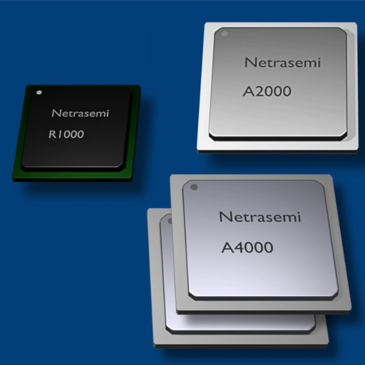
Netrasemi Brings Up A2000 AI Chip, Begins Customer Evaluation Phase
Indian startup Netrasemi has launched the A2000 AI chip built on a 12-nm technology node. Netrasemi announced it has brought up its A2000 edge AI chip and has begun supplying engineering samples along with the development platform to selected customers. The chip, manufactured on TSMC’s 12-nm process, is the first full-feature SoC developed by the startup and forms the foundation of a broader product roadmap that includes the R1000 AI microcontroller and the future R4000 chiplet-based processor. The company is currently working with early-stage customers, including OEMs and ODMs, to validate the platform and develop reference designs before moving toward production next year. In an exclusive conversation with EE Times, Jyothis Indirabhai, CEO and co-founder of Netrasemi, said, “This is a very important milestone for Netrasemi. The A2000 is our flagship chip because it contains the complete set of in-house IPs that we have developed. The successful bring-up gives us confidence in taking our entire family of SoCs to production.” You can watch the full interview below: The company is currently supplying evaluation kits (EVKs) and engineering samples to customers rather than selling production silicon to focus on validation, customer feedback, and ecosystem development. “Our objective is to ensure that the chip is tested properly and that the reference designs are ready,” he said. “Without reference designs, it is difficult to engage with OEMs and ODMs.” The company expects initial revenue by the end of next year as production begins. Netrasemi’s heterogeneous graph stream architecture Indirabhai described the A2000 as the company’s flagship product because it incorporates the full set of in-house hardware acceleration IP developed by Netrasemi. The chip delivers up to 12 TOPS of AI performance and integrates a complete video pipeline, vision processing capabilities, and a neural processor. The company said it has been designed for applications requiring AI, vision, and vector processing while maintaining power efficiency and cost targets suitable for products such as surveillance cameras. The A2000 is built on what Netrasemi calls its heterogeneous graph stream architecture. The architecture combines multiple in-house IP blocks, including neural processing units (NPUs), graphics processing units (GPUs), vector engines, general-purpose vector engines, direct memory access (DMA) engines, and encryption engines. “We developed what we call the heterogeneous graph stream architecture, which enables multiple heterogeneous algorithms to run efficiently together,” Indirabhai said. “We built the architecture and the IP portfolio first.” Jyothis Indirabhai (Source: Netrasemi) The company has also developed a software development environment called Netra Edge Studio, which includes sample applications, compiler tools, drivers, and supporting software. “We have built the studio to simplify development and reduce the effort required from customers,” he said. Indirabhai said the architecture allows multiple AI models to run simultaneously with minimal overhead. “Take the example of an in-cabin driver monitoring system that may require around six AI models operating together,” he explained. “The architecture is designed to minimize inefficiencies caused by context switching and resource allocation.” The company selected the 12-nm process node because it offers what Indirabhai described as a balance between performance and manufacturing cost. “We are targeting edge and embedded applications,” he said. “At 12 nm, we do not lose much performance while the manufacturing cost remains manageable.” Netrasemi licenses interface IPs such as double data rate (DDR), USB 3.0, and Peripheral Component Interconnect Express (PCIe), while developing its core acceleration and processing IPs internally. The company also uses Arm processors under the Arm Flexible Access program and has adopted the Shakti RISC-V core as the basis for its RISC-V development efforts. “We selected Shakti because we wanted complete control over the IP,” Indirabhai said. “We are modifying and extending it.” Future product roadmap The A2000 forms part of a larger family of processors sharing a common architecture. Alongside the A2000, Netrasemi has taped out the R1000, a real-time processing microcontroller with built-in AI capabilities aimed at IoT and smart sensor applications. The R1000 was taped out in the last week of April and is expected to return from fabrication in August. The startup described the R1000 as an ultra-low-power AI microcontroller targeting AIoT applications. “Both the R1000 and A2000 are targeted for production next year,” Indirabhai said. The company is also developing the R4000, a higher-performance chiplet-based processor built on the same architectural foundation. This chip is being positioned as an edge AI server-class chip by Netrasemi. “The neural processor architecture we developed can scale both up and down,” he said. “That is why we were able to create both the R1000 and A2000 using the same architecture. The next evolution of that architecture is the R4000.” The R4000 uses a chiplet architecture and is being developed as a two-die solution. Although the processors target different performance levels, they share common architectural components. The A2000 uses an Arm Cortex-A processor, the R1000 uses a RISC-V R25 core, and the R4000 also adopts a Cortex-A-based SoC architecture. The company’s strategy is to create a portfolio of scalable IPs and products rather than building standalone chips. Avenues for market growth Netrasemi initially targets surveillance, in-cabin monitoring, selected automotive applications, and drone-based surveillance. “These are sectors where smart vision is a primary requirement,” Indirabhai said. He added that the underlying technology can support many more applications, including media analytics, audio processing, and millimeter-wave radar processing. “We believe it can support more than 100 applications,” he said. “However, as a startup, we cannot address every opportunity simultaneously.” Netrasemi has therefore focused its interfaces, software ecosystem, and reference designs on a limited number of high-volume markets. Although the startup sees opportunities globally, India remains an important market because of local procurement advantages and growing demand for surveillance and vision-based systems. “India is an attractive market because we are a local company, and there are favorable procurement policies,” Indirabhai said. “Even in some of our market studies, India is emerging as the second-largest market opportunity for both the R1000 and R2000.” Potential customers include companies developing single-board computers, cameras, and other embedded systems, along with integrators serving industrial, automotive, commercial, and residential markets. “Camera deployments in India are growing rapidly,” he said. “If local companies do not address this market, a large volume of chips will continue to be imported.” The company currently packages its multi-project wafer (MPW) chips through overseas outsourced semiconductor assembly and test (OSAT) providers, including Kyocera, but is evaluating Indian OSAT providers for future production. Netrasemi also credits government support for helping the company reach its current stage. The company is one of the beneficiaries of the Design Linked Incentive (DLI) scheme under the Ministry of Electronics and Information Technology (MeitY). “Officials from MeitY have been involved throughout the process, reviewing progress and supporting the program,” Indirabhai said. Over the next year, the company plans to continue customer sampling, build reference designs, and gather product feedback. Depending on the results, it may undertake another multi-project wafer cycle before entering full production. “Customer feedback is more important than orders at this stage because it helps us avoid mistakes and refine the product,” he said. Netrasemi expects to secure sufficient customer commitments by the second quarter of next year to support mass production and plans to move to full-mask production by the middle of next year. Netrasemi has raised about $15 million in two funding rounds and expects to raise additional funds to support manufacturing.
Computex 2026: Are We Heading for the Agentic PC Era Yet?
Video Interview As Computex 2026 draws to a close this week, EE Times caught up with Jim McGregor, principal analyst at Tirias Research, to share thoughts on some of the key things happening during this major annual trade show in Taipei, Taiwan. You can watch the full interview below: Alternatively, you can listen to the full audio file here: Audio 3 Over the last two to three years, Computex in Taipei has been dominated by AI hype. While the conversation two years ago focused heavily on AI PCs, this year’s event shifted decisively toward agentic AI. As the CEO and founder of Nvidia, Jensen Huang, proclaimed in his opening keynote on Monday this week at the Taipei Music Center (yes, he always fills a whole stadium wherever he goes, especially in Taiwan), “Agentic AI and useful AI have arrived.” When Huang has a message, he will deliver that message in a hundred ways to emphasize his viewpoint: We are entering a new era of agentic PCs, where we interact with our PCs in a completely different way. Nvidia is framing this as an entirely new class of PCs, co-developed with Microsoft and powered by the new Arm-based Nvidia RTX Spark CPU unveiled at the show. But is it that easy? Listen to what Jim McGregor says in the video. Beyond agentic computing, this year’s event also underscored the industry-wide momentum behind physical AI, alongside a subtle but clear consensus among visiting executives: Taiwan remains the definitive epicenter of the global electronics value chain.
European Electronic Waste Dilemma
Europe has high recovery, but imperfect recycling. The global economy generated 62 million metric tons of Waste Electrical and Electronic Equipment (WEEE) in 2022, a volume that continues to accelerate alongside technological advancement. In the European Union, stringent legislative frameworks mandate the collection and recycling of e-waste. Yet, the reality of the recycling industry is complex. While a significant volume of e-waste is collected and processed, a substantial proportion is handled outside regulated channels or managed in ways that reveal how financial constraints impact recycling decisions and outcomes. Source: Global E-waste Monitor 2024 For formal operators, the transition toward a circular economy requires navigating a difficult landscape shaped by regulatory mandates, intense price competition, and global commodity fluctuations. Compliance gap and shadow economy At the ACS Recycling facility in Sabadell, Spain, operations focus on receiving, categorizing, and dismantling electronic waste sourced from across the region. In an interview with EE Times, CEO Cristóbal González Durán said the formal recycling sector faces persistent pressure from unregulated market actors. “We fight against the scrap dealer,” González Durán told EE Times, explaining that informal operators completely bypass the operational costs associated with legal and environmental compliance. Cristóbal González Durán (Source: ACS Recycling) This disparity creates a dynamic of regulatory arbitrage. Certified European recycling facilities incur substantial overhead to meet environmental, safety, and labor standards, with compliance for industry certifications such as WEEELABEX averaging €34,000 (~$39,451) annually. Informal networks, unburdened by these expenses, can offer higher immediate cash payouts for valuable electronic scrap. This practice diverts high-quality materials away from formal processors, leaving advanced plants short of the volume needed for cost-effective operations, thereby reducing their profitability and long-term sustainability. The consequences of this shadow economy extend well beyond local market distortions. Organized networks frequently exploit maritime routes to transport electronic waste to developing nations. To bypass international export bans, operators regularly declare non-functional electronics as second-hand goods. In destination countries such as Ghana and Nigeria, informal workers process these materials using rudimentary techniques, including acid baths and the open-air burning of coated cables to extract copper. These unregulated practices release persistent organic pollutants, heavy metals, and carcinogenic dioxins into the local biosphere, resulting in documented health crises, including neurological damage and elevated cancer rates among local populations. Structural pressures in the Spanish market In Spain, the electronic waste market is governed by Extended Producer Responsibility (EPR) systems, locally known as SCRAP (Sistemas Colectivos de Responsabilidad Ampliada del Productor). These organizations aggregate technology manufacturers and distributors and collect fees to finance end-of-life treatment for products placed on the national market. While intended to ensure controlled waste management, the system introduces financial pressures. González Durán describes a competitive environment where collective systems lower management fees to attract manufacturers, creating a “fratricidal war.” Image by Tung Lam from Pixabay “Between them, they steal producers by reducing quotas,” González Durán observed. When these systems lower their pricing to win corporate clients, the reduced financial compensation is passed directly downstream to the recycling facilities. As a result, recyclers are required to process larger volumes at reduced margins to maintain financial viability. In Catalonia, the regional enforcement agency, Agència de Residus de Catalunya, applies strict compliance frameworks, requiring facilities to secure an Integrated Environmental Authorization (AAI) that dictates specific emission limits and operational parameters. While the regional government allocates millions in subsidies to support recycling, operators must still contend with fierce competition over processing fees, which continues to put pressure on their financial health and operational stability. Limitations of the second-life market Before materials are mechanically shredded or smelted, facilities must assess the potential for reuse, aligning with European targets. However, the secondary market for electronics faces practical and economic barriers. González Durán pointed out that consumers typically discard devices only when they are entirely nonfunctional; functional equipment is generally sold directly to secondary markets rather than sent to recycling centers. “If the market does not buy it, you have thrown money away,” González Durán noted regarding the costs of preparing obsolete equipment for reuse. Furthermore, OEMs are often reluctant to support product refurbishment, fearing that substandard repairs will damage their brand reputation. Consequently, many corporate clients demand the physical destruction of their hardware, prioritizing data security over component reuse. Metallurgical bottleneck At ACS Recycling, components such as PCBs are sent to specialized smelters. These facilities, often traditional mining companies, use high-temperature and chemical methods to recover base and precious metals. For these industrial groups, electronic waste accounts for only a minor share of their total volume, processed alongside primary ores because the infrastructure already exists. Recovery of embedded materials depends on commodity prices. Copper, gold, silver, and palladium are routinely extracted, but the recovery of elements such as lithium and cobalt varies. According to González Durán, specialized metal-recovery processors extract these battery metals only when market prices justify the cost. “When the price of cobalt is high, it is worth it; when the price of cobalt is not, it is not worth it,” he said. If the recovery process costs more than the metal’s market value, the materials are sent to other facilities or discarded, illustrating the rigid economic limits of urban mining. Trade policy and unintended consequences In an effort to secure supply chains for critical raw materials and reduce reliance on imports, the European Union has implemented stringent regulations on the export of electronic waste. Recent legislation prohibits the export of electronic waste to non-OECD countries and increases monitoring within the bloc to retain valuable resources within the European industrial ecosystem. While the legislative intent is clear, the policy presents operational challenges for domestic recyclers. González Durán pointed out a structural imbalance in the European strategy: The continent lacks the manufacturing base necessary to consume the recovered materials. “They have prohibited it because we cannot depend on China’s supply chain,” González Durán argued. “But if we don’t manufacture here, no one is going to consume.” This policy keeps recovered metals in a market where domestic manufacturing demand is insufficient, causing smelters to offer lower prices to recyclers. As a result, recycling plants earn less from the commodities they process, tightening their margins and making it harder to sustain profitable operations. “We are all tied up here at this point,” González Durán concluded, noting that the financial strain is ultimately distributed across the entire supply chain, from the recycler to the system, the manufacturer, and eventually the consumer.
InchFab Sells $10M Mini Fabs to Democratize Chipmaking
InchFab is selling mini fabs to pharmaceutical maker Roche and universities that want to get into the chipmaking game. For an investment of about $10 million, InchFab can help customers start production of about 10,000 4-inch silicon wafers per month in as little as six months, CEO Mitchell Hsing told EE Times in an exclusive interview. The startup’s mini fabs are cost-competitive with larger 8-inch wafer fabs at the half-micron and larger nodes and offer advantages such as high-mix, low-volume production, and rapid prototyping—all difficult for large-scale chipmakers, according to Hsing. “We’ve just started to sell our lines—one in operation, several deliveries in the next 12 months,” Hsing said. InchFab came from the Ph.D. work Hsing and co-founder Parker Gould did at MIT, focused on lowering the multi-billion dollar entry barrier to making chips. The company believes its mini facilities can compete with a typical eight-inch wafer fab making 10,000 wafers per month. The cost of an eight-inch facility today ranges from $450 million to $1.5 billion, depending on production capacity, and building one takes up to five years to start production. It’s hard to fill a fab that’s running 10,000+ wafers per month and maintain profitability, according to Hsing. An InchFab unit can run much more like a memory fab, which is 100% utilized running a single process flow as opposed to running multiple process flows, he noted. Mitchell Hsing (Source: InchFab) The company has two business areas, Hsing said. “One is we provide foundry services,” he detailed. “We manufacture devices for people, just like TSMC would, or GlobalFoundries. The second thing we do is sell our manufacturing lines. We have three primary uses. One is called minimal viable manufacturing: high-mix, low-volume applications where you need specialty process capabilities for a new type of device. Typically, these are things that a foundry has a hard time manufacturing because of their specialty process.” InchFab operates its foundry in Silicon Valley. Production capacity depends on the process flow, Hsing said. InchFab foundry “We’re running one line with several customers now,” Hsing said of the foundry. “If it were optimized for a single process flow, it would probably be about 1000+ wafers per month. The reason this works is because the [production] lines are scalable. You could put in one line, two lines, three lines, four lines, five lines.” Amy Leong, a board member with chip foundry Skywater and e-beam toolmaker Multibeam, told EE Times she became familiar with InchFab at an industry event in Silicon Valley this past April. “InchFab’s ‘fab in a box’ approach has real disruptive potential,” Leong said. “By reducing prototype fab costs to under $10 million, they make semiconductor manufacturing accessible to organizations that historically couldn’t participate. For markets where volumes are low and process customization is high—specialty sensors, biomedical devices—InchFab can deliver professional-grade fabrication at a fraction of traditional cost. Beyond serving existing niches, they could also unlock entirely new markets: universities training future chip engineers, and emerging economies looking to build domestic semiconductor capability.” InchFab’s foundry customers range from universities to companies in aerospace and defense, as well as industrial sensing for oil and gas. “AR and VR applications,” Hsing added. “You can name the large companies in the AR/VR space.” Contrarian InchFab does everything that’s not logic and memory, according to Hsing. What does that leave? “Compound semi, power, quantum, photonics, MEMS, sensors, biochips, analog RF,” Hsing noted. “If you’re trying to do logic and memory, a traditional foundry route will be by far more cost effective because there are standard process capabilities out there.” InchFab’s foundry business is focused on pureplay MEMS fabrication like Silex or Atomica. “We handle lots of different types of customer-required processes,” Hsing said. “The fab in effect feeds the [production] line sales. We use our own foundry service as process development for lines that we sell.” InchFab isn’t alone in the mini fab business. Pragmatic and Nanotronics have been trying to gain a foothold. “At the moment, our sales focus is on our IDM products and our foundry offerings, and this is where we are seeing the most sales traction,” a Pragmatic spokeswoman told EE Times. Nanotronics was unavailable for comment. Hsing noted other competitors such as Minimal Fab of Japan and Atlant 3D in Europe. Hsing discounted the idea that mini fabs are only competitive for small-scale production. “As the industry reaches the end of Moore’s Law, new processes are required to maintain innovation. This is becoming the differentiator, and these processes are non-standardized and often hard to justify using high-capex fabs. Our fabs are much lower capex and as a result can maintain high utilization and therefore be competitive on price with larger wafer fabs.” The InchFab co-founder said he’s significantly cut the cost of setting up a pilot line or a university fab. He gives an example he’s familiar with: MIT.Nano, a shared, open-access laboratory space for students, faculty and industry partners. “It was a $400 million empty building,” Hsing said. “Adding in equipment gets you close to $1 billion. InchFab does all of this for orders of magnitude less.” InchFab’s production tools InchFab keeps costs low by designing and manufacturing its own production tools with a group of suppliers around the world. “Our advantages over traditional foundries in this sense are process flexibility and cycle time,” Hsing said. “The third one is cost. The reason that’s the case is because of the equipment we have that is modular, application specific, and more agile. To some extent, our foundry demonstrates that.” The company will stick with the four- and two-inch wafers that are still widely available. “Going to larger wafers will make the equipment substantially more expensive, so the advantages disappear,” Hsing said. InchFab uses laser direct-write lithography, a digital patterning method that replaces physical photomasks with a computer-controlled laser. The company also uses more traditional mask-based lithography tools. E-beam is in the future, Hsing said. Roche Pharmaceutical maker Roche, the only company that Hsing names as a customer, is making “labs on a chip” for biomedical applications. Quantum sensors are among the more esoteric devices that InchFab makes. Quantum sensors use fundamental principles of quantum mechanics—superposition, entanglement, and wave-particle duality—to measure physical quantities such as time, gravity, and magnetic fields with unprecedented precision. “Many quantum-related devices, including quantum sensors, still operate at modest wafer volumes, and InchFab offers a compelling way to shorten time to market while keeping fabrication costs manageable,” Leong said. InchFab’s mission is to democratize chip manufacturing, according to Hsing. “That’s ultimately how you enable new technology to come to market,” he said. “In today’s world, where you need multi-billion dollars to build a fab, that becomes an inhibiting step to innovation.” Still, InchFab is unlikely to win business from big companies in the chip industry, Leong said. “Their model is optimized for bespoke processes and low-volume production,” she said. “Those strengths also mean they are unlikely to attract high-volume commercial customers.”

Secure Your Supply, Accelerate Your Designs: A Practical Guide to the Memory Super Cycle
Technician working on a tablet in a data center Date: Thursday, July 9, 2026 Time 15:00 CEST The AI revolution is reshaping the memory industry, presenting unique supply challenges—such as longer lead times and allocation-based supply—and new opportunities for engineers and procurement professionals. Jointhis practical webinar where we will help you understand what’s behind these changes, what to expect next, and how to make smarter decisions around forecasting, sourcing, and design to stay ahead of the curve. Attendees will gain insight into: How the AI-driven memory super cycle is transforming industry requirements—and what it means for your business Where Infineon fits in the evolving memory landscape — and why it matters to your sourcing strategy How to identify memory solutions that fit your application and accelerate time to market with technical support and enablement resources _Not sure if you will be able to attend? No problem! All registrants will receive a link to watch the presentation on-demand after the live event._ Suggested content from our partner Arrow: More from EE Times: RELATED TOPICS:AUTOMOTIVE, COMMUNICATION, COMPUTE, INDUSTRIAL, SPACE COMPANIES:ARROW, INFINEON TECHNOLOGIES 0 comments