InchFab Sells $10M Mini Fabs to Democratize Chipmaking
InchFab is selling mini fabs to pharmaceutical maker Roche and universities that want to get into the chipmaking game. For an investment of about $10 million, InchFab can help customers start production of about 10,000 4-inch silicon wafers per month in as little as six months, CEO Mitchell Hsing told EE Times in an exclusive interview.
The startup’s mini fabs are cost-competitive with larger 8-inch wafer fabs at the half-micron and larger nodes and offer advantages such as high-mix, low-volume production, and rapid prototyping—all difficult for large-scale chipmakers, according to Hsing.
“We’ve just started to sell our lines—one in operation, several deliveries in the next 12 months,” Hsing said.
InchFab came from the Ph.D. work Hsing and co-founder Parker Gould did at MIT, focused on lowering the multi-billion dollar entry barrier to making chips. The company believes its mini facilities can compete with a typical eight-inch wafer fab making 10,000 wafers per month. The cost of an eight-inch facility today ranges from $450 million to $1.5 billion, depending on production capacity, and building one takes up to five years to start production.
It’s hard to fill a fab that’s running 10,000+ wafers per month and maintain profitability, according to Hsing.
An InchFab unit can run much more like a memory fab, which is 100% utilized running a single process flow as opposed to running multiple process flows, he noted.
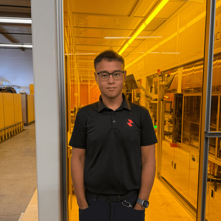
Mitchell Hsing (Source: InchFab)
The company has two business areas, Hsing said.
“One is we provide foundry services,” he detailed. “We manufacture devices for people, just like TSMC would, or GlobalFoundries. The second thing we do is sell our manufacturing lines. We have three primary uses. One is called minimal viable manufacturing: high-mix, low-volume applications where you need specialty process capabilities for a new type of device. Typically, these are things that a foundry has a hard time manufacturing because of their specialty process.”
InchFab operates its foundry in Silicon Valley. Production capacity depends on the process flow, Hsing said.
InchFab foundry
“We’re running one line with several customers now,” Hsing said of the foundry. “If it were optimized for a single process flow, it would probably be about 1000+ wafers per month. The reason this works is because the [production] lines are scalable. You could put in one line, two lines, three lines, four lines, five lines.”
Amy Leong, a board member with chip foundry Skywater and e-beam toolmaker Multibeam, told EE Times she became familiar with InchFab at an industry event in Silicon Valley this past April.
“InchFab’s ‘fab in a box’ approach has real disruptive potential,” Leong said. “By reducing prototype fab costs to under $10 million, they make semiconductor manufacturing accessible to organizations that historically couldn’t participate. For markets where volumes are low and process customization is high—specialty sensors, biomedical devices—InchFab can deliver professional-grade fabrication at a fraction of traditional cost. Beyond serving existing niches, they could also unlock entirely new markets: universities training future chip engineers, and emerging economies looking to build domestic semiconductor capability.”
InchFab’s foundry customers range from universities to companies in aerospace and defense, as well as industrial sensing for oil and gas.
“AR and VR applications,” Hsing added. “You can name the large companies in the AR/VR space.”
Contrarian
InchFab does everything that’s not logic and memory, according to Hsing. What does that leave?
“Compound semi, power, quantum, photonics, MEMS, sensors, biochips, analog RF,” Hsing noted. “If you’re trying to do logic and memory, a traditional foundry route will be by far more cost effective because there are standard process capabilities out there.”
InchFab’s foundry business is focused on pureplay MEMS fabrication like Silex or Atomica.
“We handle lots of different types of customer-required processes,” Hsing said. “The fab in effect feeds the [production] line sales. We use our own foundry service as process development for lines that we sell.”
InchFab isn’t alone in the mini fab business. Pragmatic and Nanotronics have been trying to gain a foothold.
“At the moment, our sales focus is on our IDM products and our foundry offerings, and this is where we are seeing the most sales traction,” a Pragmatic spokeswoman told EE Times. Nanotronics was unavailable for comment.
Hsing noted other competitors such as Minimal Fab of Japan and Atlant 3D in Europe.
Hsing discounted the idea that mini fabs are only competitive for small-scale production.
“As the industry reaches the end of Moore’s Law, new processes are required to maintain innovation. This is becoming the differentiator, and these processes are non-standardized and often hard to justify using high-capex fabs. Our fabs are much lower capex and as a result can maintain high utilization and therefore be competitive on price with larger wafer fabs.”
The InchFab co-founder said he’s significantly cut the cost of setting up a pilot line or a university fab. He gives an example he’s familiar with: MIT.Nano, a shared, open-access laboratory space for students, faculty and industry partners.
“It was a $400 million empty building,” Hsing said. “Adding in equipment gets you close to $1 billion. InchFab does all of this for orders of magnitude less.”
InchFab’s production tools
InchFab keeps costs low by designing and manufacturing its own production tools with a group of suppliers around the world.
“Our advantages over traditional foundries in this sense are process flexibility and cycle time,” Hsing said. “The third one is cost. The reason that’s the case is because of the equipment we have that is modular, application specific, and more agile. To some extent, our foundry demonstrates that.”
The company will stick with the four- and two-inch wafers that are still widely available.
“Going to larger wafers will make the equipment substantially more expensive, so the advantages disappear,” Hsing said.
InchFab uses laser direct-write lithography, a digital patterning method that replaces physical photomasks with a computer-controlled laser. The company also uses more traditional mask-based lithography tools. E-beam is in the future, Hsing said.
Roche
Pharmaceutical maker Roche, the only company that Hsing names as a customer, is making “labs on a chip” for biomedical applications. Quantum sensors are among the more esoteric devices that InchFab makes.
Quantum sensors use fundamental principles of quantum mechanics—superposition, entanglement, and wave-particle duality—to measure physical quantities such as time, gravity, and magnetic fields with unprecedented precision.
“Many quantum-related devices, including quantum sensors, still operate at modest wafer volumes, and InchFab offers a compelling way to shorten time to market while keeping fabrication costs manageable,” Leong said.
InchFab’s mission is to democratize chip manufacturing, according to Hsing.
“That’s ultimately how you enable new technology to come to market,” he said. “In today’s world, where you need multi-billion dollars to build a fab, that becomes an inhibiting step to innovation.”
Still, InchFab is unlikely to win business from big companies in the chip industry, Leong said.
“Their model is optimized for bespoke processes and low-volume production,” she said. “Those strengths also mean they are unlikely to attract high-volume commercial customers.”