Industry News
The latest news on the semiconductor and electronic-parts industry .

Rebellions Bets on Memory-Centric Architecture as it Weighs IPO Options
South Korean AI silicon startup Rebellions is focusing its technology roadmap on memory as it seeks to take advantage of strategic connections with Korean semiconductor giants SK Hynix and Samsung Foundry. The company believes this strategy will be crucial as it explores options for an IPO, Rebellions CEO Sunghyun Park told EE Times. “Rebellions, as a Korean startup, backed by Samsung and SK Hynix, is in a very good position to explore all the options for memory-centric architectures,” Park said. Sunghyun Park (Source: Rebellions) As large-scale LLMs reach deployment, memory capacity and bandwidth are becoming critical to large AI inference accelerator designs like Rebellions’. The company’s second-generation AI accelerator, Rebel, was announced in 2024. Rebel is a scaled-up version of Rebellions’ first-gen CGRA-based accelerator, with four compute chiplets offering 1 POPS of FP16 compute and 144 GB of HBM4e in a 300-W power envelope. Memory is therefore of extreme strategic importance, in terms of both supply chain and economics. The industry is moving away from commodity memories in a number of directions, Park said. Huge KV caches will require a combination of HBM and HBF (high-bandwidth Flash) for capacity, while scale-up and scale-out solutions will require specialized memory architectures and memory pooling. The industry is also exploring custom HBM implementations. The company had planned a 3D SRAM stack for its next-generation architecture, but has switched to 3D-stacked DRAM as part of a collaboration with both SK Hynix and Samsung. Park said Rebellions is working to co-design HBM memory and logic dies; custom HBM could include logic to handle fast token decoding, but the industry is still figuring out which logic to include. “There’s no de facto standard solution yet, so it’s a good time to explore what options we can have in the base die for custom HBM,” he said. Customer base Rebel is commercialized primarily in South Korea and the Middle East today, Park said. Having secured its memory supply chain, Rebellions is receiving significant attention in the Kingdom of Saudi Arabia (KSA) in particular. “Everyone talks about technology, but the most important thing right now is to secure the supply chain,” he said. “The beauty of Rebellions is we can secure all the memory.” Turbulence in the Middle East of late hasn’t dampened the region’s AI infrastructure ambitions, Park said. “Humain is still the same, Aramco is still the same,” he said. “They believe [AI] is not just a trend. It’s their ambition for 2030, and I’m proud to be part of the ecosystem here in Saudi Arabia.” Groq was the main player in this region until recently, Park noted, and changes there have brought the Middle East closer to the Korean ecosystem in search of other hardware candidates. “Sovereign AI [in KSA] means a heterogeneous compute platform where Nvidia and non-Nvidia hardware co-exist, and where U.S. and non-U.S. hardware are installed together,” he said. “Training and inference are not locked in by Nvidia products here, and [we have] a very compelling story.” As well as sovereign deployments, telecoms is the other key market for Rebellions, both in the Middle East and South Korea. “The telecoms industry has money, and they know how to do capex,” Park said. The biggest deployment of Rebellions chips to date is at SK Telecom, where a multi-rack first-gen Rebellions cluster partially powers Adot, SK Telecom’s proprietary AI assistant, which provides Korea-specific services like summarizing phone calls. Adot is the biggest user of tokens in South Korea, Park said, with up to 50 million API calls per day. The companies are currently exploring options for scale-up and scale-out of this cluster. “I’m proud that we have end users for this service; it’s not just infrastructure, it’s a real, live service in Korea,” he said. Rebellions hardware is also deployed in NPU-as-a-service infrastructure by Korea Telecom (KT). Rebellions’ open-source software stack, optimized for Red Hat, is popular with potential U.S. customers, but this is still a growing market for the Korean company, Park said. Rebellions’ hardware has been deployed at both SK Telecom and Korea Telecom. (Source: Rebellions) Chiplet architecture AI silicon startup Cerebras’ huge IPO last month has put new price tags on companies like Rebellions, Park said, and brought investor and customer focus to low-latency inference, which is further intensifying focus on memory technologies and supply chain. While the first big exits in this domain, Groq and Cerebras, both have SRAM-based architectures, the next big winners will be those who use 3D DRAM stacking, Park said. “One year ago we focused on chiplets; chiplet was the magic word,” he said. “Today, the magic word is memory and memory-centric architectures. That’s why [we are getting traction] with financial investors, because we’re uniquely positioned here.” Rebellions recently taped out CXL and Ethernet I/O dies, but plans to sell compute chiplets are still evolving. The industry landscape around chiplets is still moving, Park said, so it’s too soon to decide whether chiplets are a valid go-to-market option for a startup. “Who’s my friend and who’s my enemy in this field?” he said. “Even Nvidia is trying to build its own chiplet ecosystem. Right now, I don’t know what direction [we’ll go in]. I’d like us to be the chiplet player for XPU, but we need to find the right partners and the right packaging partner. It’s very important to understand what’s going on in this ecosystem.” The company collaborates with Marvell on system-level technologies, including optical scale-up (Rebellions is considering co-packaged optics for future generations, Park said, to keep up with customer demands for bigger scale-up domains). Both the AI chip companies that had big exits recently had moved even further up the stack, building out substantial cloud deployments of their own. Would Rebellions consider doing something similar? “It’s an option,” Park said. “API service is good because we can hide all the numbers by abstracting the customer [further] from our silicon, but frankly, we don’t have a specific direction yet because we are still figuring out the tokenomics.” The Korean government has encouraged Rebellions to build its own sovereign data centers, but that would require additional investment, Park said. Rebellions hardware can be used alongside GPUs for decode acceleration, but it can also handle prefill perfectly well, Park said. (Source: Rebellions) The trend for disaggregated inference, where inference workloads are split across different types of more specialized chips, has been amplified by the Nvidia-Groq deal. Park said that while the industry doesn’t yet have a standard approach to disaggregation, Rebellions is working with Arm and SK Telecom on a disaggregation project. In this specific setup, Rebellion’s hardware accelerates the decode stage; Rebellion’s compute chiplets have significant SRAM, in some ways similar to the Groq chip in Nvidia’s disaggregated architecture. “It’s an interesting idea, and the collaboration between Arm, SK Telecom, and Rebellions is working well, but I’m not sure whether disaggregation is the right overall direction in the future,” he said. Rebellions’ current-generation chip, Rebel, has HBM, Park added, so it can also easily handle prefill. Rebellions closed a $400 million pre-IPO round in March, bringing total funding raised to $850 million. The company is talking with its bankers, Park said, but no concrete plans have been made for the IPO just yet. The company is exploring both Nasdaq and domestic listing options, Park said, while another strategic funding round pre-IPO is also an option.

GigaDevice Introduces GD32E512 and GD32E252 MCUs for Optical Modules
Singapore (June 11, 2026) — GigaDevice, a leading semiconductor company specializing inFlash memory,32-bit microcontrollers (MCUs),sensors, andanalog products,has introduced the new GD32E512 and GD32E252 series MCUs specifically designed for optical module applications. As a leading supplier of MCUs for optical module applications, GigaDevice has maintained a strong focus on the optical communication market, continuously aligning its product development with evolving industry requirements and next-generation optical interconnect technologies. Leveraging years of expertise in optical module control solutions, GigaDevice has established a strong position in the market through continuous innovation and close collaboration with industry partners. To further support the advancement of high-speed optical interconnect technologies and expand its optical communication product portfolio, GigaDevice has introduced the new GD32E512 and GD32E252 series MCUs specifically designed for optical module applications. The new products extend GigaDevice’s optical communication MCU portfolio, addressing the diverse requirements of both high-speed and low-speed optical modules while providing highly integrated and application-optimized solutions. Backed by its comprehensive technology portfolio spanning Flash memory, MCUs, analog devices, and sensors, GigaDevice offers fully self-developed and mass-production-ready solutions with high reliability, strong performance, and flexible customization capabilities for a wide range of optical module applications. Eight Years of Innovation in Optical Module MCUs Through continuous technology investment and product innovation, GigaDevice has become one of the key MCU suppliers serving the global optical module industry. As a leading manufacturer of 32-bit general-purpose MCUs, while steadily expanding its business across multiple sectors, GigaDevice’s in-depth advancement in the optical module segment has always kept pace with the evolution of global communication technologies. In 2018, the company made forward-looking investments in the R&D of optical module MCUs and launched its first dedicated MCU, marking a technological breakthrough. It quickly achieved million-unit shipments within the same year of product launch. Driven by dividends from advancing communication technologies and the ongoing refinement of its product portfolio, GigaDevice’s shipments of optical module-specific MCUs hit the ten-million-unit mark in 2022, ranking among the world’s top players and securing full coverage of mainstream optical module and equipment customers at home and abroad. Amid the booming growth of AI computing power and surging demand for high-speed interconnection, GigaDevice GD32 MCUs are now fully compatible with core application scenarios including telecom, data centers, and access networks. The company is further focusing on three cutting-edge technological directions: high-speed pluggable optics, silicon photonics, and and co-packaged optics (CPO)., continuously empowering the industry’s transition to next-generation high-speed networks. GD32E512 Series: Designed for High-Speed Optical Module Applications Targeting the demanding requirements of high-speed optical modules,the GD32E512 series features a high-performance Arm Cortex®-M33 core operating at up to 120 MHz. The series introduces integrated I3C support, enabling high-bandwidth, low-latency, and high-density communication to meet the evolving requirements of next-generation optical modules. The GD32E512 series is available in an ultra-compact 3 × 3 mm package, helping customers optimize PCB space and support the ongoing trend toward higher integration and miniaturization in optical module designs. To further simplify system design, the GD32E512 series integrates a rich set of application-oriented peripherals, including 3× I²C, 1× MDIO, 2× ADC, 4× DAC, 2× comparators (COMP), and 2× operational amplifiers (OPA), providing comprehensive monitoring, control, and management capabilities for high-speed optical module applications. GD32E252 Series: Optimized for Low-Speed Optical Module Applications The GD32E252 series is specifically designed for low-speed optical module applications and is built around the Arm Cortex®-M23 core. Through continuous optimization, the series delivers enhanced analog performance while maintaining a high level of integration, low power consumption, and reliable operation. Designed to address the requirements of access networks, industrial optical communications, and other cost-sensitive optical connectivity applications, the GD32E252 series provides an optimized balance of performance, integration, and efficiency. The devices also feature compact package options, wide-temperature operation, and strong EMC performance, helping customers simplify system design, reduce development complexity, and accelerate time-to-market. Enabling the Future of High-Speed Optical Connectivity The introduction of the GD32E512 and GD32E252 series further expands GigaDevice’s optical communication MCU portfolio, providing optimized solutions for both high-speed and low-speed optical module applications. Together, these products address the evolving requirements of AI data centers, cloud infrastructure, telecommunications networks, and access networks. Looking ahead, GigaDevice will continue to invest in optical communication technologies and expand its application-focused MCU portfolio. Supported by a broad semiconductor product ecosystem and a reliable global supply chain, GigaDevice remains committed to enabling next-generation optical interconnect solutions and supporting the continued growth of AI computing, cloud services, and high-speed networking infrastructure. About GigaDevice GigaDevice Semiconductor Inc. is a global leading fabless supplier. Founded in April 2005, the company has continuously expanded its international footprint and established its global headquarters in Singapore in 2025. Today, GigaDevice operates branch offices across numerous countries and regions, providing localized support at customers’ fingertips. Committed to building a complete ecosystem with major product lines – Flash memory, MCU, sensor, and analog – as the core driving force, GigaDevice can provide a wide range of solutions and services in the fields of industrial, automotive, computing, consumer electronics, IoT, mobile, networking, and communications. GigaDevice has received the ISO26262:2018 automotive functional safety ASIL D certification, IEC 61508 functional safety product certification, as well as ISO9001, ISO14001, ISO45001, and Duns certifications. In a constant quest to expand our technology offering to customers, GigaDevice has also formed strategic alliances with leading foundries, assembly, and test plants to streamline supply chain management. For more details, please visit: www.gigadevice.com _GigaDevice, GD32, and their logos are trademarks, or registered trademarks of GigaDevice Semiconductor Inc. Other names and brands are the property of their respective owners._ COMPANIES:GIGADEVICE SEMICONDUCTOR INC 0 comments
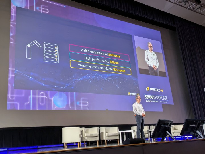
RISC-V Targets Data Centers, Edge AI, Space
As RVA23 becomes globally adopted RISC-V open architecture reaches server maturity. BOLOGNA, Italy — For years, RISC-V open-standard instruction set architecture worked quietly behind the scenes, mostly appearing in microcontrollers, hard drives, and specialized industrial applications. But at this week’s RISC-V Summit Europe 2026 in Bologna, the message to the global tech community was unequivocal: The architecture has matured and now targets data centers, edge AI, and space exploration markets. “RISC-V is now,” said Andrea Gallo, CEO of RISC-V International, during his opening keynote address to a full auditorium. Gallo’s speech showed that RISC-V is close to major commercial growth. According to the SHD Group, RISC-V could reach 33.7% market share across all hardware segments by 2031. (Source: RISC-V International) This growth is especially visible in edge computing and data centers, with markets expected to top $45 billion and $70 billion by the end of the decade. The hardware ecosystem is booming, as startups such as SiFive and Axelera have raised $650 million together, and big companies such as Microsoft are joining as top board members. Year of RVA silicon in the data center A key moment for RISC-V’s use in business came with the official ratification of the RISC-V Server Platform Specification 1.0, based on the RVA23 profile, ratified in 2024. This important step standardizes the hardware, bringing industry-standard boot systems and runtime services, such as UEFI and ACPI 6.6 support, directly to RISC-V. It ensures that system software runs smoothly across different server hardware. “It’s really important because it’s bringing industry standards to RISC-V,” Gallo noted in an interview with EE Times following his keynote. “At the same time, it’s the industry standards that are supporting RISC-V because the ACPI 6.6 officially supports RISC-V now.” This strict standardization is already driving a surge in high-performance chips. Called the “year of the RVA silicon,” 2026 is seeing many companies launch new server-class processors. Both large companies and startups are releasing powerful hardware, such as the SiFive Performance P870D with up to 128 cores, Akeana’s Alpine Test Chip, and NextSilicon’s Arbel server-grade CPU. Source: RISC-V International Epic Semi has launched its Contrail AIX, a superchip that blends 32 RISC-V processor cores with 16 built-in AI cores, reaching up to 75 TOPS. “The server platform is the completion of the first phase,” Gallo explained during the interview. “Starting from RVA23, the server SoC, and then the server platform. And then this incredible number of RVA23 high-performance chips are coming out all this year. This is incredibly exciting for us.” Andrea Gallo (Source: RISC-V International) For hyperscalers and data center operators, RISC-V is a strong alternative to proprietary architectures such as ARM and x86, effectively mitigating the risk of single-vendor lock-in. “The market is so large that there’s room for everyone,” Gallo said. “So it’s not that one is displacing the other, but there’s enough room for everyone for RISC-V to grow into the market.” He stressed that having choices is important for multinational companies and governments working on digital sovereignty. “RISC-V is bringing freedom of choice and freedom from a single vendor,” Gallo added. Big software companies have noticed this change. Canonical’s new Ubuntu 26.04 LTS operating system now fully supports RVA23, making it easier for enterprise teams to manage data centers with diverse hardware. Addressing physical AI at the edge Enterprise servers are a huge market, but the rise of AI is just as transformative. Gallo sees the future going beyond text and image recognition, toward “physical AI” that interacts directly with the real world. “The evolution that we see is that AI initially was inference, so it was recognizing,” Gallo told EE Times. “Then it became agentic, making decisions. And the physical means that you are also activating those decisions in the physical world.” To make physical AI work—whether in a robot adjusting its balance or in remote sensors deployed in the Amazon rainforest—the hardware must use very little power. RISC-V does this with advanced vector and matrix extensions, letting complex AI algorithms run on the same core that handles control software and the operating system. This design approach removes the need to constantly transfer data and weights to a separate neural processing unit, avoiding a slow, power-hungry process known as “memcopy.” “You don’t do memcopies to transfer the data, the weights from the CPU to the NPU, but everything is done on the same core,” Gallo said. “Memcopy means latency because it takes time, and memcopy means power consumption.” By removing this internal data-transfer problem, RISC-V greatly reduces power consumption and enables much smaller chips. This advantage was clear in Beijing, where a humanoid robot using SpacemiT’s K3 RISC-V processor finished a half-marathon. In Brazil, researchers at São Paulo University are using locally made, battery-powered RISC-V microcontrollers to build an “Internet of Trees.” This mesh network can automatically detect illegal logging and forest fires. Reaching the final frontier in space exploration Beyond Earth applications, RISC-V is becoming a key part of the next generation of spaceflight computers. Space is harsh, requiring microprocessors that are highly radiation- and fault-resistant. Historically, the aerospace industry relied heavily on legacy SPARC-based architectures, but an industry-wide pivot to RISC-V is now well underway. To organize this effort, a special RISC-V Space Special Interest Group started at the end of 2025, chaired by representatives from the European Space Agency and E4 Computing. The group was created because the industry needed to adapt the open architecture for space. “Everyone had some questions,” Gallo recalled from a previous space workshop. “How do we configure RISC-V at best for the lunar lander? Or how do we configure RISC-V at best for cloud processing on a satellite? How do we properly isolate the software workloads on a satellite?” Now, the group brings together experts from NASA, Microchip, SiFive, and Frontgrade Gaisler to write strict standards and white papers for these specialized space missions. Major hardware projects are already underway. NASA is working with Microchip and SiFive to test a high-performance spaceflight processor, and the European Commission’s COSMIC7 project is building a 7-nm RISC-V chip designed just for orbit. For older aerospace suppliers such as Frontgrade Gaisler, now moving from SPARC-based LEON processors to new RISC-V-based NOEL chips, the open nature of RISC-V is the main attraction. Aerospace groups need full transparency in their hardware to get safety certifications. “There’s a strong requirement for publicly available specifications for them to be able to own the product, to own their destiny,” Gallo said. “RISC-V is the only alternative to natural evolution.” Mature ecosystem and commercial success The RISC-V ecosystem is evolving quickly, with both strong startup growth and increasing participation from major companies. Gallo sees this as proof that the architecture works. “When you have such successful acquisitions, it means that those companies were doing things really right,” Gallo said, noting the steady stream of new startups launching high-performance chips. The developer community is just as enthusiastic. At RISC-V Summit Europe 2026, developer workshops sold out, with 120 engineers working on hands-on debugging and advanced hardware design challenges. People no longer see RISC-V as just an academic project or a simple embedded controller. The open architecture has clearly matured, supported by standard specs, strong corporate support, and a large software ecosystem. It is now ready for applications ranging from enterprise computing and edge AI to the demanding environment of spaceflight. As Gallo said at the RISC-V Summit Europe 2026, the tech industry no longer needs to ask when RISC-V will arrive. It is already here.
Logistics Leaders Navigate Cost and Automation
Gartner’s VP analyst David Gonzalez shares strategies for profitability and technology in supply chain management. BARCELONA, Spain— Supply chain operators are facing more pressure from unpredictable shipping costs, higher customer service expectations, automation, and ongoing labor shortages. As chief supply chain officers work to keep things running during global disruptions, logistics is changing in fundamental ways. In an interview at the recent Gartner Supply Chain Symposium/Xpo, David Gonzalez, VP analyst at Gartner, told EE Times that the industry needs to focus on careful cost management, practical technology, and updated infrastructure. He described important changes that will help logistics support business growth. (Source: Gartner) Imperative for profitability David Gonzalez (Source: Gartner) “Logistics has always been challenged with cost optimization but high standards of service delivery,” Gonzalez said, noting this is a constant expectation in the field. But as consumer demand grows, companies risk losing profit. “Customer expectations are increasing, but you have to do it profitably as well,” he said. Gonzalez emphasized that logistics services must not operate at a loss. He recommended that companies use strict cost-to-serve and cost-to-deliver models. This requires operators to carefully assess the tradeoffs of premium services, such as same-day delivery, and the investments needed to provide them. Logistics leaders and company decision-makers need to communicate openly to keep costs under control. Gonzalez said logistics managers should be honest with executives about the real costs of their requests. “Maybe sometimes logistics leaders need to share that information to say, yes, I can deliver whatever it is you want me to deliver, but are you prepared to spend money on that level of expectation?” he said. Executives often keep service levels consistent or use customer segmentation to match delivery costs to product value. Logistics leaders have to decide if they can pass costs on to customers or cover them with product margins. “If the answer is no, then logistics leaders should ask whether we should do this at all,” Gonzalez said. Visibility of the supply chain As global supply chains become increasingly complex, reliable shipment tracking is more important than ever. Gonzalez pointed out that manual methods are no longer enough. “Emailing spreadsheets back and forth for visibility doesn’t work anymore,” he said, given the growing number of disruptions facing the industry. However, he warned companies not to overspend on tracking technology without a clear plan. Organizations must decide if they need to track products, truck locations, or broader information. A detailed, constant tracking like big e-commerce platforms offer. “One customer said, ‘I want the Amazon experience—updates every few minutes on my driver’s location,’” he recalled. Gonzalez responded by warning about the costs. “Be careful what you wish for… Are you ready to spend what Amazon did for that level of tracking?” He suggested only alerting managers about delays or problems, instead of tracking everything all the time. Pragmatism in AI adoption Despite a focus on AI, logistics lags other enterprise areas in adopting it. Gartner reports that only about 13% of logistics leaders have fully implemented AI, trailing manufacturing, planning, and supply chain strategy. Gonzalez sees this slow adoption as a sign that the sector is practical. “Whether that illustrates a healthy dose of skepticism on the part of logistics, or whether we are still too focused on the physical execution of logistics, I’m not sure,” he said. Gonzalez recommended starting with small projects that solve specific problems, instead of trying to overhaul all technology at once. He mentioned Unilever’s use of agentic AI to handle daily questions about orders, trucks, and containers. The system answers questions, tracks exceptions, and finds relevant data. “Because of that, productivity for Unilever’s logisticians rose by 50%,” Gonzalez said. He said this kind of targeted investment is a smart approach and warned that buying technology without a plan can waste money fast. Workforce reality and automation Gartner predicts that by 2030, half of the new warehouses in developed markets will be ‘robot-centric,’ making human labor optional. “AI continuously optimizes warehouse environments in real-time, shifting them from static structures into agile systems that adapt as demand changes,” said Abdil Tunca, senior principal analyst in Gartner’s supply chain practice. Source: Adobe Stock This aligns with Gonzalez’s view that demographic shifts are driving companies toward greater automation. “Necessity is going to be the mother of acceleration rather than invention in logistics,” he said, pointing out that fewer young people want jobs in warehouses or as truck drivers. Advanced humanoid robots remain costly and face challenges such as heavy batteries, but traditional industrial robots are already widely used. The main challenge is making everything work together. Gonzalez said the industry should update its equipment, instead of trying to fit robots into old spaces. “Maybe we need to adapt our infrastructure to accommodate the capabilities of the robot,” he suggested, pointing out that warehouses and vehicles may need to be redesigned. Operators should plan for a decade ahead where human pickers are scarce, thereby altering infrastructure “to the reality of the future rather than the other way around.” Shift from standardization to customization Changing consumer needs make it harder to adapt infrastructure. In the past, logistics depended on uniform systems. “We standardize everything—pallets, containers—for efficiency,” Gonzalez explained. But direct-to-consumer delivery requires more customized handling. “You’re asking an industry to go from a high degree of standardization to a high degree of customization,” Gonzalez said. “And the transition is the struggle.” This problem is reflected in automated centers struggling to handle unusual items and excessive packaging. Gonzalez cited a longstanding industry example to illustrate the limitations of today’s robots when handling oddly shaped items. “The robot can very easily pick the perfect box, but how does it pick these things that are cumbersome and inconvenient and challenging?” he asked, pointing to the challenge of automating the handling of a canoe. Figuring out how to handle these physical challenges remains a big obstacle as the industry moves toward more automated and customized logistics networks. See also: Suggested content from our partner Arrow: More from EE Times: RELATED TOPICS:AUTOMATION, HUMANOID ROBOTICS, LOGISTICS, ROBOTICS, SUPPLY CHAIN, WAREHOUSE COMPANIES:GARTNER _Pablo is a seasoned engineer with 30+ years of experience. For over 10 years, he's been a contributing editor for EE Times (now editor of the Supply Chain section). He also wrote for EPSNews, InformationWeek, EBN, LightReading, Network Computing, and IEEE Xplore. His coverage spans Supply Chain, Semiconductors, Networks, IoT, Security, and Smart Cities. He holds an MEng, Electrical and Electronics Engineering from The Ohio State University._Follow Pablo on LinkedIn 0 comments

Startup Ricursive to Create an End-to-End AI Model for Chip Design
PALO ALTO, Calif. — Startup Ricursive, founded by the two leads from Google’s famous AlphaChip project, aims to develop an end-to-end AI model for chip design. The new AI frontier lab is focused on hardware workload co-optimization, with the first stages of its rollout targeting workload-specific chip design for third parties. The company has raised $335 million, which will largely be spent on GPU compute hours as it trains and tests its model. In an exclusive interview with EE Times, Ricursive co-founder and CEO Anna Goldie, as well as co-founder and CTO Azalia Mirhoseini, stressed that the startup is not an EDA company, will not compete with EDA companies, and will not utilize standard EDA toolchains. Azalia Mirhoseini (Source: Ricursive) “What we are doing is different [to EDA], we are doing end-to-end chip design,” Mirhoseini said. “We want to transform the chip design industry, such that we can enable a new platform that can make chips for any customer that doesn’t have their own teams of chip experts in-house, but has an algorithm that they are serving at scale. We can make the chips for them such that they can do so significantly more efficiently than using an off-the-shelf chip.” Goldie and Mirhoseini have been working together for 10 years, starting the machine learning persistence team at Google Brain, one of whose projects was AlphaChip. AlphaChip, developed in 2018, was heralded as one of the first reinforcement learning (RL) approaches used to solve a real-world engineering problem. It was used for macro placement across four generations of Google TPUs and was adopted externally by chip companies, including MediaTek. “What we’ve done in this company goes way beyond [AlphaChip] in terms of the breadth of what we’re taking on in the chip design flow, the performance improvements we can achieve, and the speed of the way, way higher,” Goldie said, confirming that Ricursive will not license or use any Google IP. Google had offered to make an Alphabet spinout for the pair to continue their work on AlphaChip and related projects, Goldie said, but it seemed like a middle ground. “We love Google, we grew up there, Google feels like home,” she said. “[But] we’ve had more resources here [at Ricursive], we’ve had more focus here, we’ve had much higher velocity here.” Ricursive wants to help build chips beyond Alphabet, and that requires being an independent company, Goldie said. “We wanted to have that broader impact,” she said. “We also thought that as a standalone company, not only would other chip makers trust us more and know that they can send us their data, but we also thought we can move faster, because we have this company whose [entire] mission is to accelerate this process and close this loop. That’s never really existed before.” Now is the perfect time to start an AI company, Mirhoseini added, since the needs of the industry, combined with the state of AI technology, are creating the perfect opportunity. End-to-end design Ricursive has planned three stages for its technology rollout. The company is currently working on phase one. In this phase, Ricursive will take on portions of chip design for chip companies, improving performance and helping companies get to market faster. “The goal in phase one is to accelerate the chip design process, basically, to take on the long pulls, physical design, and design verification,” Goldie said. “We believe that if you don’t accelerate both of those, then you can’t accelerate the process end-to-end. And we think it’s really, really important to be able to move more quickly from architecture to GDSII that you can actually implement.” Anna Goldie (Source: Ricursive) Phase two will combine the stages of chip design into an end-to-end model that can ingest workloads and spit out GDSII files ready for manufacturing. It will enable fast, custom chip designs, which are particularly useful in AI accelerators given the scale of their deployment, but can be applied across any workload. “Our thesis is that if we customize the compute architecture to the model architecture, we can achieve massive performance improvements, but we can only unlock that performance if we can quickly implement that architecture,” Goldie said. “It can’t take a year or two to do that, or it would be obsolete.” Ricursive also wants to democratize chip design for companies that have at-scale workloads but have not previously considered custom hardware. Ricursive will do the design work for them using its AI and foundry relationships to help customers get custom chips across the line. This could apply to chips for scientific discovery and healthcare workloads, such as DNA sequencing, Mirhoseini said. “We may not need those applications at scale, but we could enable them,” she said. “By lowering the cost and the time that it takes [to build a chip], we can have more applications, not just be more efficient, but potentially even enable applications that otherwise wouldn’t have been possible because of their latency or power requirements.” Hardware-workload co-design Phase three is the ultimate vision for Ricursive, in which model, workload, and hardware are tightly co-designed. “If we have this capability to quickly build highly performant chips, why not build our own chips, train our own models, and co-evolve them?” Goldie said. “Frontier models are about the tradeoff of cost versus capability, and we think we can be on a totally different Pareto-optimal curve through the co-evolution of chips and models.” Ricursive’s models will be generally intelligent (not just for chip design), so the eventual chip will also apply to more general AI workloads. The intention is for AI to eventually handle everything from chip design to system and infrastructure design—the entire stack. “In the third phase, we want to make a frontier AI, period,” Mirhoseini said. “Why not co-evolve the chips and AIs together? This is not an AI for chip design, this is just AI.” This is similar to what OpenAI and Anthropic are doing, Mirhoseini said, noting that they handle code generation, math, and language with the same model. Mirhoseini was on a team that originated the original mixture-of-expert models; the eventual Ricursive model could follow this structure, with a common level of intelligence that supports different specialties, she said. “The way we think about phase three is that the chips are enablers of models,” Mirhoseini said. “If you can co-evolve the chip and model together, you can speed up training time by multipliers, you can speed up your explorations in post-training and RL by a multiplier. That means the inner loop of designing this new model can be sped up by a multiplier. That’s how it enables the AI to evolve faster. That’s how we are thinking about chips as the catalyst for self-improvement and evolution.” Ricursive is training its model on generally available web data and open-source chip data, but can also create and use synthetic data to avoid hitting the limits of what is available in the real world today. Advanced AI models need less data, Goldie said, since knowledge can transfer across tasks. Ricursive is also working with chip companies to demonstrate early results on their real chip designs and get their feedback. This is valuable since open-source data is not representative of real designs, Goldie said. While hardware-workload co-design is happening to some extent today, Goldie said it is extremely slow. Researchers working on new model architectures have to think about what runs quickly on today’s hardware, while chip makers have to think about what will be prevalent in two to three years. “It’s a deadlock,” she said. “We want to tighten that loop dramatically.” A faster end-to-end flow will enable a spectrum of custom chips and enable new applications, Goldie said. “Long term, we believe we’re at a local optimum,” Goldie said. “We have these chips that are pretty good, but we think the global optimum is potentially a very different computer architecture, and a very different neural architecture, and we want to find that.”

Massive AI Storage Demand Creates a New Memory Wall
The term “Memory Wall” was coined in the early 1990s to describe a bottleneck in computer performance: the speed gap between processors and memory, specifically DRAM. The premise quickly insinuated itself into the engineering vernacular with DRAM cast as a laggard technology dragging computing efficiency. That wall remains, but in the AI era, the metaphor takes on a new meaning as DRAM and DRAM-based high-bandwidth memory (HBM) strive to meet the skyrocketing memory needs of large language models (LLMs). Over the past 30 years, DRAM has met performance scaling requirements through innovative techniques such as cache hierarchies, prefetching, and memory interleaving. Designers developed larger and faster on-chip caches and introduced techniques to predict and pre-load data before it was needed. However, these techniques did not solve the fundamental issue of capacity scaling. Today’s rapidly expanding AI models are placing an unprecedented strain on the ability of conventional memory architectures to expand capacity ahead of data storage demand. The signs are everywhere—rising DRAM and HBM design and manufacturing costs, higher energy use and heat dissipation, and diminishing scalability options. AI inference modeling redefines data retrieval patterns and priorities The constraints placed on DRAM-based memories, such as HBM and graphics double data rate (GDDR), come as LLMs expand from billions to trillions of parameters. At the same time, AI inference context sizes—driven by complex prompts, retrieval-augmented generation (RAG), chain-of-thought reasoning, and user-specific data—often require key value (KV) caches larger than the models themselves. The DRAM architecture used today as system memory is less relevant in AI inference workloads, which are predominantly read-heavy and latency-tolerant due to predictable memory access patterns that enable prefetching and buffering. This renders HBM’s narrow focus on raw bandwidth insufficient for workloads requiring both capacity and bandwidth. These challenges underscore the need for new memory architectures that optimize capacity and bandwidth specifically for AI inference. Rather than relying on consistent, cache-friendly access patterns, AI inference models process highly variable and multidimensional data types. The AI inference memory accesses are deterministic, prefetch-friendly, and feature a large granularity. All of this makes caching hierarchies less relevant than raw sequential bandwidth. The resulting AI computing paradigm succeeds not by brute-forcing memory bandwidth but by optimizing when and how data is retrieved. In this context, it enables the use of alternate memory technologies tailored for high capacity and sequential bandwidth as a smarter way to address this problem. The new memory challenge becomes optimizing a mosaic of flowing data as opposed to a linear increase in speed. Historically, data center designers addressed the lack of balance between compute and memory capacity needs by partitioning and distributing AI inference workloads across multiple, expensive accelerators. This technique often wasted computing capacity, but the added cost and power consumption were justified when amortized across large data centers with large user bases whose requests could be processed in large batches. It was only when distributed processing was applied to smaller enterprises with limited user bases, or to large data centers serving disparate customers, that batching became inefficient. A new approach to AI memory As AI inference workloads grow in scale and complexity, high-bandwidth flash emerges as an alternative. Unlike DRAM and HBM, which are costly, power-hungry, and capacity-limited, high-bandwidth flash leverages the high-density advantages of NAND flash. By using stacking techniques and wafer bonding, such as CMOS directly bonded to array (CBA) technology, these emerging architectures demonstrate higher memory capacity than HBM. While high-bandwidth flash latency is higher than DRAM, AI inference workloads are increasingly bandwidth-bound rather than latency-sensitive. These new memory designs exploit high-density NAND-based technology tailored to deliver high bandwidth for large-granularity read operations through concurrent accesses across multiple arrays of memory cells. This makes them suitable for LLM storage and read-intensive inference. In these high-bandwidth memory usage environments, high energy dissipation makes thermal stability at high temperatures a very important requirement. High-bandwidth flash, based on NAND technology, is potentially more stable and better suited for these environments than DRAM. Non-volatility and enhanced endurance versus standard NAND flash also position high-bandwidth flash for persistent KV cache data to be reused to mimic long-term memory. As AI computing demands continue to grow, relying solely on DRAM and HBM may limit architectural innovation. High bandwidth flash offers data center and edge AI designers a scalable, efficient memory alternative tailored to the evolving needs of AI, where performance is no longer determined by latency but by the efficiency of inference-driven data orchestration. Resources: McKee, S.A., Wisniewski, R.W. (2011). Memory Wall. In: Padua, D. (eds) Encyclopedia of Parallel Computing. Springer, Boston, MA. https://doi.org/10.1007/978-0-387-09766-4_234 Read also: Relief is coming. The three companies that control virtually all of the world’s DRAM production are investing at a scale the industry hasn’t seen in decades. The harder truth is that those fabs come online in 2027 at the earliest, with meaningful relief unlikely before 2028. RELATED TOPICS:AI INFERENCE, DRAM, HIGH-BANDWIDTH MEMORY, LARGE LANGUAGE MODELS, MEMORY WALL, SEMICONDUCTORS, STORAGE COMPANIES:SANDISK _Alper Ilkbahar is CTO and executive VP of memory technology at Sandisk, overseeing NAND technology development, next-generation technologies, corporate research functions, and market development._ 0 comments
AI-Driven Memory Shortage Upends IT Budgets
According to Gartner, RAM shortage and price spikes have increased server costs by over 125% in the first half of 2026. As the rapid buildout of AI infrastructure continues to consume massive volumes of advanced memory, corporate IT departments and OEMs are confronting a crippling structural shortage of DRAM and NAND flash components. This crisis has made enterprise budgets unpredictable, yet it has also brought record profits to the world’s top memory manufacturers. Margin boom for memory makers Driven by explosive demand from cloud service providers for enterprise solid-state drives and high-capacity memory, top-tier semiconductor companies are reporting historic revenue growth. In the first quarter of 2026, market research firm TrendForce said the top five global NAND flash suppliers saw their combined revenue jump 83.7% from the previous quarter, reaching over $38.9 billion. This growth is driven primarily by higher prices resulting from the shortage, rather than by increased production. According to TrendForce, Samsung maintained its market lead during this period, reporting $13.51 billion in NAND flash revenue, a 104.7% increase from the previous quarter. SK Hynix and Kioxia also saw big gains, with their revenues rising by 44.6% and 80%, respectively. Micron Technology and SanDisk shared fourth place in market share, and both saw their revenues rise 96.7% from the previous quarter. By focusing on high-value, high-capacity products for businesses, these companies have protected their profits, even though higher costs have slowed down demand for smartphones and personal computers. Navigating the supply squeeze For corporate buyers and equipment makers, these high profits for manufacturers mean it is much harder to buy what they need. According to Gartner, in the first half of 2026, memory prices have increased by 50% to 200%, driving server costs up by more than 125%. Because of the shortage, equipment makers have had to change or even cancel server setups that need a lot of memory. Source: Gartner In an email exchange with EE Times, James Smith, senior director analyst at Gartner, warned that regular negotiation tactics no longer work for corporate IT buyers. Vendors now issue price quotes valid for only a week, and many can raise hardware prices right up until they ship the products. To handle this unstable market, Smith recommended that companies change how they buy memory. Even though the shortage may last until at least 2027, he warned against panic buying or signing strict contracts. James Smith (Source: Gartner) “The real risk is turning a forecast into a fixed take-or-pay commitment before the market settles,” Smith said. “In our research, we recommend building 12- to 24-month demand forecasts, not locking buyers into long-term purchase commitments.” If buyers start discussions early and share updated forecasts with suppliers, they can give vendors the information they need without locking themselves into high prices. Companies should make actual purchase commitments monthly or quarterly, rather than annually. “Our recommendation is to signal demand early, stay close to suppliers, and preserve flexibility until supply and pricing become more predictable,” Smith added. Immediate production relief is an illusion Even though memory manufacturers are investing heavily, there is no quick fix for the supply shortage. TrendForce analysts said that major NAND flash suppliers will not add much new production capacity in 2026. Instead, they are using their current resources for the most profitable server storage products. Well-publicized expansions of domestic manufacturing are aimed at long-term changes, not at quickly increasing supply. Micron Technology recently started making its 1-alpha DRAM at its Fab 6 facility in Manassas, Virginia, which federal lawmakers praised as a win for U.S. supply chain security. Micron said its $2 billion expansion in Virginia will eventually enable it to quadruple DDR4 memory production in the U.S., but industry analysts pointed out that this is really just shifting capacity around the world. TrendForce research shows that Micron is moving its older memory production from Taiwan to Virginia to serve industries such as defense and automotive, as well as other long-term uses. This change lets Micron’s Taiwan factories focus only on making the newer DDR5 and high-bandwidth memory (HBM) needed for AI. As a result, the total global supply of standard LPDDR4 and DDR4 memory will stay about the same, so the shortage is likely to continue. Addressing these industry developments, Smith noted that buyers must manage their expectations. “The supplier investments now underway are positive, but they do not automatically mean broad near-term relief,” Smith explained. Prioritizing workloads and sourcing Since new hardware is still hard to find and costly, IT supply chain leaders have to reconsider when to upgrade and explore other ways to obtain equipment. Gartner suggests delaying non-essential purchases and using the secondary market, such as leasing devices that can have their memory upgraded. Because older hardware from the secondary market cannot meet the performance demands driving the AI boom, Smith emphasized the need for strict workload triage. “Fundamentally, yes, reliance on the secondary hardware market can contradict the performance demands driving the current AI boom,” Smith explained. “But for most organizations, that is not the whole story.” He clarified that standard end-user computing and core operational tasks do not strictly require premium, AI-ready infrastructure. “Older servers, especially those that can take memory upgrades, can still support lower-priority and keep-the-lights-on workloads,” Smith noted. “That is not a contradiction so much as a prioritization strategy to reserve premium infrastructure for workloads that genuinely need it.” Cloud pricing pass-throughs are not the solution The financial ripple effects of the hardware shortage are now extending beyond physical servers and into software and cloud services. As data center infrastructure costs rise, software-as-a-service and infrastructure-as-a-service providers are beginning to pass these costs on to their enterprise customers. However, Smith insisted that supply chain leaders must aggressively scrutinize these rate hikes. “Vendors should not be allowed to blame the economy and expect customers to simply accept higher prices,” Smith argued. He advised corporate buyers to demand empirical evidence that their specific usage or workload profile has materially changed, rather than accepting price hikes based on the vendor’s hypothetical future capacity expansions. “Resistance isn’t refusal; it is just challenging the vendor to justify their demands,” Smith said. “If the workload is essentially unchanged, customers should resist footing the bill for broader market shifts or for investments that primarily benefit other customers.” In the end, enterprise buyers need to stay flexible and cautious to handle the current memory market. Since supply problems may last through 2027 and manufacturers are benefiting from the shortage, business leaders should focus on careful forecasting, clear workload priorities, and strong negotiation to get through this crisis.

India’s 2035 Chip Ambitions Focus on Targeted Design, Manufacturing Leadership
In this video fireside chat, EE Times’ senior India correspondent explains how the local ecosystem is evolving and what she hears on the ground in India. In May 2026, India’s public policy think tank NITI Aayog published Future of India’s Semiconductor Industry, a 65-page report detailing the strategy for building a $120 billion to $150 billion semiconductor value chain by 2035. The report lays out a roadmap centered on areas considered critical to India’s economic growth and strategic autonomy, including mature-node logic, specialty analog and mixed-signal chips, and compound semiconductors such as silicon carbide and gallium nitride. The report highlights that India should play to its strengths in chip design talent, a skilled workforce, and the potential of its materials and chemistry ecosystem. It states: “Building on these advantages, it should aim to emerge as a global leader in semiconductor design and system architecture, a top-three destination for outsourced semiconductor assembly and test (OSAT) and advanced packaging and a trusted supplier of critical semiconductor materials, particularly wide-bandgap and advanced packaging materials. In these domains, India should aspire to set standards, shape supply chains and create enduring global dependence, rather than limit itself to mere participation.” EE Times has covered India for years with what would appear as many false starts over those years. So, are the latest initiatives any different, and what kind of results can we expect? To find out, we caught up with our senior India correspondent, Yashasvini Razdan, in Delhi, India, at the end of last month about what she has been seeing and hearing from her reporting for EE Times over the last 18 months. In this fireside chat, she explains why this effort appears different from previous attempts and what it could mean for India’s semiconductor ambitions. Watch the complete video conversation here: In the conversation, Razdan covers India’s shift from assembly to product development, various overlapping government incentives and schemes such as the India Semiconductor Mission, some of the smart commercial manufacturing strategies such as the focus on mature nodes and why that matters for India’s market, and global geopolitical alliances such as Tata and ASML. She also highlights grassroots efforts to develop talent and promote inclusivity, including expanding early access to technology for students and increasing opportunities for women in the industry.

Rethinking the Logic-Routing Tradeoff in FPGAs
Efinix has launched a family of FPGAs aimed at edge AI applications, based on soft or hard RISC-V cores with instruction extensions for AI. The Titanium Edge family outperforms other FPGAs on performance, power, and economics, Bob Beachler, corporate VP of marketing and corporate development at Efinix, told EE Times. Efinix’s secret sauce is in its XLR logic cell. Traditional FPGAs have to balance how much silicon space is dedicated to routing and how much is available for logic; FPGA companies have made logic blocks more complex to minimize routing, since routing is expensive in terms of area, Beachler said. But once data has to move outside a logic element, it has to be driven down wires, which consumes power and contributes to thermal stress. “For some sets of designs, the ratio [between logic and routing] is wrong, you either have too much routing and waste silicon area, or you have too many logic elements that you can’t route to,” he said. “In a typical FPGA design, you may have places that have lots of routing but are very congested, and some areas of the design that don’t need as much routing as they are very sparse.” Efinix’s key IP is around enabling its logic cell to do either logic or routing (XLR stands for exchangeable logic and routing). “In that way, we can dynamically determine how much routing or how much logic goes into each area of a given design,” Beachler said. Software determines how much logic and routing is required, and where. “This is very efficient,” Beachler said. “This technology can have similar or greater performance than top-performing FPGAs, but at half the power and half the die area.” Efinix’s logic cell can be used as either logic or routing, allowing the balance to change for different parts of the design. (Source: Efinix) The company has already commercialized this technology in its Titanium family, which is aimed at applications that require more processing power. The new Titanium Edge family has the same basic architecture with a few tweaks. Static power consumption has been reduced by half compared to earlier Titanium parts. Efinix has added single-event upset (SEU), post-quantum security, and higher-speed I/O. Enhanced high-speed interfaces support up to 2.5 Gb/s MIPI interfaces for image sensors. MIPI blocks in earlier Titanium parts were hardened blocks, but since the FPGA fabric is fast enough, it can be run as a soft controller, Beachler said. “This gives customers more flexibility about where they put their MIPI interfaces,” he said. Up to eight lanes of MIPI are supported. This is key to applications such as robotics, where each hand or finger contains multiple sensors. Competitive landscape AI co-processors have had limited success in the edge market, Beachler said, while SoC solutions with on-board NPUs have fared better. Successful SoC solutions typically include other accelerators such as image signal processors or video codecs. “I have customers who use both FPGAs and [off-the-shelf SoCs],” he said. “If they get a new sensor that can’t go directly into the SoC or something more custom is required, they’ll use an FPGA instead. We have IP blocks that can run video encode and decode, for example, and it will work out a little more expensive than the SoC, but it will give the designers flexibility.” FPGAs are sometimes used as front-end processing before handing off to an SoC, Beachler said. For example, humanoid robots may require processing close to the sensor before passing metadata to a bigger processor or “brain” elsewhere in the body. Co-packaged HyperRAM Efinix will offer some members of the Titanium Edge family co-packaged with HyperRAM (a DRAM die that behaves like SRAM). This can be used to store intermediate weights during AI inference or data, such as intermediate video frames. Area is drastically reduced by moving memory into the same package as the FPGA, Beachler said. “We buy the dies from Winbond, and we put them all in the package so customers can get to market faster, and they don’t have to worry about sourcing memory, which can be a big issue,” he said. “Customers love it.” Some Titanium Edge parts have two HyperRAMs, some have one. Other FPGA makers cannot stack memory dies on the FPGA die because they burn too much energy; Efinix’s energy efficiency directly enables 3D stacking, Beachler said. Some parts in the Titanium Edge series are already shipping, with the rest of the family expected to become available by the end of 2026.

The Concerning, Unchecked Rise of E2E AI in Physical Applications
The recent Artemis II moon mission was a monumental engineering achievement—perhaps humankind’s greatest ever—on many levels: It travelled farther from Earth than any other manned spacecraft, it used the most powerful rocket ever built, and it provided a shot in the arm for NASA’s ambitious goal of landing humans on Mars. But it pales in comparison to an even more ambitious engineering goal here on the ground—the frenzied push for developing fully autonomous land vehicles as the first step on the road to a robot-populated future. Artemis represents the apotheosis of the tried-and-true approach of “deterministic” engineering, or rules-driven engineering. The environment is extreme but known, failure modes are well-defined, and orbital mechanics, thermal loads, and rocket thrust are governed by equations that were originally developed hundreds of years ago by the likes of Newton and Kepler. In contrast, the emerging approach is born of recent developments in AI. It could be called “probabilistic” engineering, or end-to-end, data-driven engineering. Probabilistic, data-driven engineering learns from examples. Feed a neural network enough data, and it discovers patterns no human engineer would have thought to encode. This is a genuinely powerful and significant development. For perception-heavy tasks in open environments—such as navigating autonomous vehicles on city streets—it is often the only tractable approach. An autonomous system can’t just calculate; it must adapt and generalize in a way that rule sets cannot. You cannot write a rule for every conceivable situation: A child chasing a ball, garbage blown into the road, a faded lane marking in rain, an irate driver behaving irrationally—these scenarios are effectively infinite in variety. Probabilistic systems are powerful but inherently risky. They produce outputs by selecting from an internal distribution of possible output states. But distributions have edges, and at those edges—however rarely encountered—the output of a neural network can be catastrophically wrong. In software, a catastrophic failure corrupts data. In a physical system connected to actuators, it kills people. How we got here: the end-to-end revolution The pursuit of end-to-end AI-based vehicle autonomy was likely catalyzed by a seminal 2016 Nvidia paper, “End-to-End Learning for Self-Driving Cars.” The idea was radical in its simplicity: Instead of decomposing driving into separate modular activities—perception, prediction, planning—with carefully hand-crafted interfaces between them, simply train a single neural network to map raw sensor inputs directly to steering commands. Let the network figure out everything in between. The authors’ conclusion: “A small amount of training data from less than a hundred hours of driving was sufficient to train the car to operate in diverse conditions, on highways, local, and residential roads in sunny, cloudy, and rainy conditions.” Tesla, already the world’s largest collector of real-world driving data, applied this paradigm at scale and has refined it through successive generations of full self-driving (FSD) software. The appeal is irresistible: An end-to-end system trained on millions of hours of human driving data can, in theory, handle situations that no finite rule set could ever anticipate. Today, this direct mapping from raw sensory input to low-level control actions—pixel-to-torque—is a distinct paradigm that has gained significant momentum from the success of large language and vision-language models and is being exported to humanoid robots and surgical automation systems. The logic is the same: collect enough data, train a large enough model, and the network learns to operate the body or the scalpel. But there is a problem. The evidence is in: Tesla’s FSD—the first end-to-end AI system to be deployed at scale in uncontrolled physical environments—is not working as advertised. It’s not anywhere near achieving the level of autonomy needed for widespread acceptance and ultimately for profits. There is no clearer proof of that than Tesla’s use of remote human drivers who can take charge of Tesla robotaxis in certain cases. “As a redundancy measure in rare cases … remote assistance operators] are authorized to temporarily assume direct vehicle control as the final escalation maneuver after all other available intervention actions have been exhausted,” said [Karen Steakley, Tesla’s director of public policy and business development. That is not autonomy; it is a tacit admission that the neural network’s generalization has limits that can’t yet be trained away. The incident reports pile up. FSD vehicles failing to yield to school buses. Robotaxis driving into flooded streets. Near-misses with emergency vehicles. Former Tesla AI trainers have recently spoken on record to Reutersabout the internal pressure to ship software that engineers privately regarded as unsafe. The regulatory and legal machinery is struggling to keep up with a deployment pace driven not by safety milestones but by investor expectations. Each one of these failures is a natural experiment in what happens when a probabilistic core is connected directly to physical actuators without an adequate deterministic backstop. The experiment is being run on public roads, with real people, without their informed consent. The deterministic shell: What it is and why it matters The solution is not to abandon machine learning. It is to stop deploying it naked. A deterministic shell is a rules-based safety layer that wraps the probabilistic core. It can take several forms. The simplest may take the form of an output filter: a certified module that receives the neural network’s proposed command—steer hard left, accelerate, extend the surgical tool—and checks it against a formal specification of safe behavior before passing it to the actuator. If the proposed command falls outside the safe envelope, the filter blocks it and substitutes a safe default. The filter does not need to understand why the network made a bad decision. It only needs to know what outputs are permissible. A more robust approach could add an independent parallel monitoring system with its own physically separated sensor stack—sensors that share no hardware with those feeding the neural network, so a particular sensor failure cannot corrupt both systems simultaneously. This watchdog would run a formally verified model of safe behavior and could override the primary system if it detects an impending violation. A third layer is graceful degradation: When the monitoring system detects a failure, it does not merely sound an alarm. It executes a safe-stop maneuver autonomously, buying time for human intervention. Yes, this adds cost. It adds complexity, and it is harder to build than a bare end-to-end network. That is precisely why it has not been built—not because it is impossible, but because it is expensive and time-consuming, and the market is not yet demanding it loudly enough. The “bodies” are the market signal that has been suppressed. Harder problems have already been solved Lest anyone argues that wrapping probabilistic AI in deterministic constraints is technically intractable, consider what engineers have already accomplished. The field-effect transistor is a quantum mechanical device. At the level of individual electrons, its behavior is irreducibly probabilistic. Yet the digital logic built on top of billions of transistors is, for practical purposes, perfectly deterministic—because circuit architects designed the system so that quantum-level noise does not propagate to logic-level errors. Deterministic behavior was engineered in. It did not emerge spontaneously. Claude Shannon proved that you could transmit information with arbitrarily low error probability over a noisy, probabilistic channel by adding carefully chosen redundant bits. The noise is not eliminated. It is contained by a deterministic structure wrapped around a probabilistic medium. The intellectual tools to build hybrid architectures—probabilistic learning cores constrained by formally verified safety layers—are already in the engineering canon. The challenge is application, not invention. Elon Musk and his ilk would dismiss such guardrails as unnecessary. Musk’s position is essentially this: more data + bigger model = safety problem solved. The deterministic shell, in his worldview, would be a temporary crutch until the core is capable enough to not need it. But a recent Anthropic blog post disagrees. Anthropic’s research into large-scale AI deployment has flagged what it describes as the “hot mess” problem: models that perform coherently within their training distribution but degrade unpredictably when inputs shift. Across all tasks and models, the longer that the models spend reasoning and taking actions, the more incoherent their errors become. The harder the problem, the more the model reaches for extended reasoning, and the more incoherent it becomes, concludes the post, directly contradicting Musk’s “bigger is better” theory. The case for a deterministic shell grows stronger. A direct message to engineers This essay ends where it should: with the people who build these systems. Engineers are, in a very real sense, the last technical checkpoint between an untested probabilistic system and the human beings who will interact with it—often without understanding what it is, often without any meaningful ability to opt out. The passenger in the robotaxi did not review the training data. The patient on the surgical table did not audit the inference pipeline. They trusted the system because an engineer signed off on it. The pressure to ship is always intense. The competitive dynamics are brutal. The investors are impatient, and the deadlines are immovable. It is easy to rationalize: The edge cases are rare, the next training run will fix it, the system is already better than a human driver. But “better on average than a human driver” is not a safety standard. It is a marketing claim. A safety standard is a provable bound on worst-case behavior. Engineers should note the difference and build to the standard, not the claim. The tools exist. The precedents exist. The knowledge exists. The transistor engineers did not say “quantum tunneling is probably fine.” Shannon did not say “the channel is usually clean enough.” They built the shell. They did the hard work. They gave us reliable digital systems out of irreducibly noisy physics. What also exists—right now, on roads and in operating rooms and in robot warehouses—is a mass experiment running on unconsenting human subjects. And the error rates are measured in lives. Read also:

XENSIV™ TMR-based Sensors: Unlocking New Possibilities in Magnetic Sensing
Magnetic sensing is becoming increasingly important in modern electronic systems, particularly in motion control, power conversion, and protection applications, where contactless measurement of position and current is essential. These signals directly influence control quality, system efficiency, and how quickly protection mechanisms can respond. Across consumer, industrial, and automotive domains, designs are moving toward smaller form factors, faster switching and control loops, and higher accuracy requirements. However, these trends introduce new challenges. As systems shrink, the available magnetic signal becomes weaker. Faster operation increases susceptibility to electrical noise, while tighter performance targets leave less margin for error. Tunnel magnetoresistance (TMR) technology addresses these challenges by combining high sensitivity, low noise, and strong intrinsic signal output, enabling reliable sensing even under demanding conditions[1]. This article introduces the fundamentals of TMR sensing and shows how Infineon applies this technology in practical solutions for accurate and robust magnetic field measurement. Application examples include position sensing in compact user interfaces, coreless isolated current sensing for power conversion and motor drives, and ultra-fast overcurrent protection in high-voltage solid-state systems. Together, these examples demonstrate how Infineon’s XENSIV™ magnetic sensor based onTMR portfolio[2] enables scalable, high-performance sensing solutions across consumer, industrial, and safety-relevant applications. Table of contents 1. Why magnetic sensing is evolving in modern systems Magnetic sensing in modern electronic systems enables contactless measurement of motion (position or angle) and electrical load (current). It is becoming increasingly relevant wherever compact designs, electrification, and fast electronic control converge. In consumer devices such as gaming accessories and wearables, magnetic sensors deliver precise and consistent user input,for example in joysticks, triggers, and key switches,while supporting low-power operation. They also enable power-efficient system behavior, such as detecting inactivity and switching devices into lower-power modes, thereby extending battery life. In industrial and power applications,including power tools, drones, and energy storage systems,magnetic sensing enables accurate, contactless measurement of rapidly changing currents. This improves motor control and enhances the efficiency of power conversion systems. In protection systems such as solid-state relays, smart circuit breakers, and battery management systems, current sensing enables fast detection of abnormal conditions, allowing systems to respond quickly and prevent damage. In automotive and other safety-critical motion control systems, magnetic sensors are widely used for position and angle measurement, supporting reliable closed-loop control and enabling diagnostic functions that enhance system safety. Across these domains and many beyond, the need for improved sensing performance is driven by three key trends: 1. Size:Smaller designs and tighter packaging reduce available magnetic signal and increase sensitivity to variation 1. Speed:Faster switching wide bandgap technologies and control loops require higher bandwidth and low-latency sensing 1. Accuracy:Stricter control targets and safety requirements reduce acceptable margins for error and drift These trends introduce a common set of challenges: Detecting weaker signals in compact designs Maintaining stable measurements in electrically noisy environments Responding quickly enough for control and protection tasks Ensuring reliable performance without extensive calibration or compensation TMR technology directly addresses these challenges by providing high sensitivity, low noise, and strong output signals. By improving signal quality at the source, it reduces reliance on complex external signal conditioning and enables compact, scalable high-performance sensing solutions. 2. Understanding magnetic sensing technologies in system design Magnetic sensing technologies form the interface between physical signals and system-level decision making. As system requirements become more demanding, understanding how different sensing principles behave at the device and system level becomes critical for selecting the right solution. 2.1Overview of magnetic measurement principles Magnetic sensing technologies can be broadly grouped into Hall-effect and magnetoresistive(MR) approaches. Hall-effect sensors convert magnetic fields into voltage signals through charge-carrier deflection and provide robust, cost-effective solutions for general sensing tasks. Magnetoresistive technologies, which include anisotropic magnetoresistance (AMR), giant magnetoresistance (GMR), and tunneling magnetoresistance (TMR), convert magnetic field changes into resistance variations, enabling higher sensitivity and improved resolution. Among these, TMR offers particularly strong signal output and superior signal-to-noise ratio(SNR)[2]. Figure 1: Magnetic sensing technology overview and comparison (FL: Free Layer, TB: Tunnel Barrier, RL: Reference Layer, AF: Anti-Ferro Magnet, PL: Pinned Layer, NML- Non-magnetized layer) At the device level, TMR sensors rely on a structure consisting of two ferromagnetic layers separated by a thin insulating barrier. Changes in the magnetic field alter the relative alignment of the magnetization directions in the free and reference layers, resulting in a measurable change in resistance. At the system level, this stronger intrinsic signal and lower noise are critical advantages, because they reduce the need for external amplification and filtering while improving robustness in compact and electrically noisy environments. While these characteristics define the fundamental advantages of TMR as a sensing technology, their practical impact depends on how the sensor is operated within a system. In real applications, TMR sensors are configured differently depending on whether the goal is to extract directional information, such as angle, or to measure the magnetic field strength directly. This distinction leads to the two primary operating modes of TMR sensors,saturation mode and linear mode,which are discussed in the next section. 2.2Saturation vs. linear operation in TMR sensors TMR sensors can be configured based on whether the application needs field direction (angle) or field strength (linear measurement). Angle sensors measure sine and cosine angle components with monolithically integrated magnetoresistive elements. In linear measurement for power systems, XENSIV™ TLI5572 for example[6]is used as miniature linear magnetic sensors for coreless current sensing of bi-directional AC and DC currents. This difference (see Table 1) is significant at system level because the key design priorities differ between angle and linear sensing. Table1.Angle (direction) sensing vs. linear field measurement in MR/TMR sensors 2.3Infineon’s XENSIV™ Vortex-based TMR structures: Improving linearity and cross-field robustness In compact and densely integrated systems, the limiting factor for sensing devices is often not raw sensitivity, but how consistently they behave when real-world disturbances occur. This applies across a wide range of applications, including compact interfaces such as gaming controls, wearables, and other space-constrained designs. Cross-fields, mechanical tolerances, and limited magnetic headroom can all translate into non-ideal output behavior and unit-to-unit variation. These challenges are particularly relevant for linear-mode sensing, where the output must follow the absolute magnetic field strength and is therefore more sensitive to disturbances. Conventional TMR structures offer only a limited usable linear range, which has historically constrained robust linear sensing. Figure 2: Magnetic sensing technology overview and comparison (FL: Free Layer, TB: Tunnel Barrier, RL: Reference Layer, AF: Anti-Ferro Magnet, PL: Pinned Layer, NML- Non-magnetized layer) Vortex-based TMR addresses this by forming a stable closed-flux magnetization structure, enabling a more controlled and predictable response to external magnetic fields. This results in: Wider usable magnetic range up to ±100 mT[2] Improved linearity, with errors below 0.5% in relevant applications Significantly reduced cross-field sensitivity, with up to 100× improvement Stable output behavior, minimizing hysteresis and discontinuities These characteristics are critical in compact sensing environments, where mechanical variation and external interference can affect measurement accuracy. At the same time, they enable reliable linear-mode operation forcurrent sensing applications, where accurate field-proportional measurement is essential. 2.4 Monolithic CMOS + TMR integration: Enabling compact, application‑ready sensing While vortex structures improve linear sensing at the device level, practical system performance depends on how effectively the sensing signal is processed and integrated into the signal chain. In many designs, the sensing element is only part of the challenge. The larger system effort lies in maintaining signal integrity through PCB routing, switching noise, interface constraints, and integration into control or protection logic. This is especially critical in linear-mode sensing, where the signal depends directly on magnetic field strength. A key development addressing these challenges is Infineon’smonolithic CMOS + TMR integration, which brings sensing and signal-processing functions together on a single die. By integrating more of the signal chain into the sensor itself, this approach reduces the need for external circuitry and improves robustness. At the system level, this enables: improved signal integrity through shorter internal signal paths reduced external amplification and filtering requirements increased robustness to noise and environmental variation more compact and efficient system design. Taken together, these developments enable TMR technology to translate into application-ready sensing solutions.Table 2 provides an overview of the latest products, an extension of Infineon’s XENSIV™ TMR-based magnetic sensors portfolio across key domains and system-level requirements[2]. Table2.XENSIV™ TMR sensor portfolio for key application domains For more detailed product information and reference designs, explore the XENSIV™ current sensors selection guide and XENSIV™ magnetic position sensors selection guide. 3. Enabling high-performance sensing in applications with TMR Modern electronic systems rarely use sensing as a stand‑alone function. In motor drives, robotics, battery-powered tools, and power conversion stages, sensor outputs directly feed control and protection loops that must remain stable under fast transients and electrically noisy conditions. In these environments, improving signal quality at the sensing point is often the most effective way to reduce downstream complexity and preserve accuracy across operating conditions. These capabilities are closely linked to advances in linear-mode TMR sensing discussed in Section2, which enable accurate and robust magnetic field measurement in real-world environments. The following examples are illustrative rather than exhaustive, highlighting where TMR-based sensing brings tangible system-level value across industrial, consumer, and safety-relevant applications. 3.1Position sensing in compact interfaces (gaming and wearables) Compact input devices,especially gaming controllers and wearables,have less mechanical space, tighter power budgets, and higher expectations for consistent feel over lifetime. In these geometries and form factors,small displacements and packaging constraints can introduce unwanted magnetic field components, which may lead to non-ideal transfer behavior such as drift in center position or inconsistent actuation. 3 a) Figure 3a: a) Joystick/thumb-stick sensing can be realized either with two 1D sensors for X/Y tilt (e.g., XENSIV™ TLI55910/50) or with a single 2D TMR sensor for integrated X/Y tilt (XENSIV™ TLV552D) (Top) 3 b) Figure 3b:Functional block diagram of a gaming controller architecture (Down) In gaming and PC-peripheral designs, XENSIV™ TLI55910/50 linear magnetic devices are commonly positioned for thumb‑stick and joystick sensing, while XENSIV™ TLI55910 is also referenced for applications such as mouse click or press detection. Both XENSIV™ TLI55910 and TLI55950 are associated with keyboard single-key sensing and other compact input interfaces. More broadly, these sensing approaches extend to wearable devices where low power and stable operation are important considerations. At the device level,XENSIV™ TLI55910 enables a high-sensitivity, low-power linear TMR position sensor suited for battery-powered devices and stable operation in harsh environments, while XENSIV™TLI55950 sensor builds on this by offering an amplified output, enabling higher signal levels and improved signal usability in high-sensitivity applications[1],[5],[2]. Feature-to-benefit summary Low power and compact integration: XENSIV™ TLI55910 linear sensor is highlighted with ~0.25 mA current consumption and a compact SOT23 package, supporting battery-powered gaming interfaces and wearables where low power and space matter. Linearity and cross-field robustness: XENSIV™ TLI55910/50 sensors are high SNR analog 1D TMR sensors with high linearity and cross-field robust behavior enabled by Vortex TMR technology. A separate storyline summary also emphasizes Vortex TMR delivering superior linearity and strong cross-field robustness for consistent performance. Amplified-output option(when more signal level is needed): XENSIV™ TLI55950 is a linear TMR sensor with amplified output and is associated with high sensitivity and ultralow noise. The selection guide also lists example target applications such as power tool trigger detection, service robots and drones angle sensing, and high-precision dual-encoder setups. Design recommendation Lowest power / smallest footprint:useXENSIV™ TLI55910 linear sensor Consistency in compact mechanics:use XENSIV™ TLI55910/50 linear sensors (Vortex TMR) for better linearity and cross‑field robustness Higher output signal needed:useXENSIV™ TLI55950 linear sensor(amplified output) The same need for compact, repeatable sensing also shows up in many industrial joystick and operator-control designs, making these approaches relevant beyond consumer devices. Use cases:thumb-stick/joystick, key-switch, wearables, industrial control interfaces, mouse press 3.2 Coreless current sensing for power and motion systems(power tools, robotics,fans,energy) Fast-switching power stages and compact motor drives are placing increasing demands on current sensing: higher di/dt, stronger electromagnetic interference (EMI), tighter space constraints, and limited thermal headroom. In these environments, sensing accuracy and response speed directly affect system performance. Coreless magnetic current sensing addresses these challenges by keeping the sensing element physically separate from the current path. This enables contactless, galvanically isolated current measurement without introducing insertion losses, while still maintaining accuracy across a wide current range. High bandwidth supports fast control loops, and low-noise behavior helps ensure stable operation under electrically noisy conditions. Figure 4: Coreless current sensing with XENSIV™ TLx5572 current sensor on an external current rail: analog output (AOUT) routed to an MCU ADC for fast control and monitoring These requirements are particularly relevant in industrial energy and power conversion systems,including PV inverters and energy storage,where current measurement directly influences system efficiency, control stability, and protection response. In closed-loop motor control, current feedback determines torque response and overall system stability. This makes bandwidth, noise, and latency practical design constraints,especially in compact drives and fast-switching power conversion stages. Coreless sensing approaches help address these needs by combining isolation with the bandwidth and signal quality required for reliable, high-speed control loops. In humanoid robot actuators, external‑rail current sensing can serve as a practical alternative to shunt-based approaches. Magnetic TMR current sensors mounted above external current rails enable a compact, isolated, and low‑loss method for in‑phase current measurement, supporting efficient and responsive motion control in high‑dynamic actuator systems. In typical implementations, the sensor output is routed as an analog signal (AOUT) to an MCU’s ADC for control and monitoring, as illustrated in the XENSIV™ TLx5572 application diagram. Feature-to-benefit summary High-dynamic current feedback: XENSIV™ TLI5572 current sensor devices enable coreless current sensing for bi-directional AC/DC measurement in applications with fast current changes[6] Application focus: Used in power tools, robotics, industrial pumps & fans (motor control), AC compressors, induction cooktops and fast-switching GaN/SiC power stages and converters (e.g. in server, telecom rectifier and photovoltaic) Key capabilities: Support isolated current measurement from PCB-level to >kA, with MHz-class bandwidth, low-noise analog output, and operation from −40°C to 150°C. Scalability and efficiency: One sensing concept can scale from PCB traces to busbars, while avoiding insertion losses and parasitic inductance. Precision and system integration: XENSIV™ TLI5570 current sensor adds overcurrent detection support, configurable sensitivity, and functional safety alignment (ASIL B as SEooC)[7]. Design recommendations Fast control loops / high dynamics:useXENSIV™ TLI5572 current sensor(bandwidth, isolation, low noise) Scaling across power levels:use XENSIV™ TLx5572 current sensor approach from PCB to busbar Precision / safety features needed:considerXENSIV™ TLI5570 current sensor External‑rail sensing:validate geometry early Use cases:Cost-efficient motor drives in power tools, robotics, pedelecs and drones; fast-switching GaN/SiC drive stages and power conversion; scalable platforms from PCB-level currents to busbar-level currents; external-rail sensing concepts for robotics actuators validate via simulation workflows; PV inverters and energy storage systems. 3.3Overcurrent protection in solid-state systems (eFuse, solid‑state relay, smart circuit breaker) Figure 5: Generic block diagram of DC SSCB Solid‑state protection turns fault handling into a timing problem: overcurrent must be detected quickly and the power path interrupted before damage propagates. This is particularly relevant in high‑voltage(HV)solid‑state protection and power distribution systems such as HV eFuses and solid‑state circuit breakers (SSCBs), where current sensing and protection logic must remain reliable in fast‑switching environments.Figure 5 illustrates a generic DC SSCB architecture to provide system context[8]. Feature-to-benefit summary Integrated sensing and protection: XENSIV™ TLE5571 current sensor combines coreless TMR current sensing with integrated overcurrent detection (OCD), enabling fast response times required in protection applications. Differential measurement for robustness: The device uses two integrated TMR full bridges for differential field measurement, improving stability in electrically noisy environments. Bandwidth for fast transients: With a minimum bandwidth of 2.5 MHz, the sensor supports fast transient detection in SiC/GaN-based systems with high switching speeds. Efficiency-oriented system behavior: Coreless sensing avoids additional resistance and parasitic inductance, supporting efficient system operation while reducing the risk of false OCD triggering. Implementation context: The HV eFuse reference design positions XENSIV™ TLE5571 sensor within a high-side switching architecture, supported by design documentation covering snubber/pre-charge, control logic, and auxiliary power supply integration Implementation context: The HV eFuse reference design positions XENSIV™ TLE5571 sensor within a high‑side switching architecture, supported by design documentation covering snubber/pre‑charge, control logic, and auxiliary power supply integration. Design recommendations Fast overcurrent detection in HV protection: Use a coreless current sensor with integrated OCD and differential measurement, as represented by XENSIV™ TLE5571 sensor in eFuse/SSCB architectures. Fast‑switching, high power density environments: Select devices with MHz‑class bandwidth and minimal parasitic impact to handle rapid transients in SiC/GaN systems. Use cases:HV eFuses, solid-state relays, smart circuit breakers / solid-state circuit breakers, and HV power distribution protection systems requiring fast fault detection in fast-switching environments. 3.4Safety-oriented position sensing (automotive and industrial drives) Safety-relevant motion control relies on position sensors that support functional-safety concepts and maintain reliable angle feedback in applications such as electric power steering (EPS). If angle feedback becomes inaccurate, the control system can apply incorrect assist torque, potentially affecting vehicle stability. To meet these requirements, redundant sensor architectures are used. Single-die devices such as XENSIV™ TLE5501 achieve ASIL D through diagnostic coverage and internal redundancy (fail-safe operation), while dual-die solutions such asXENSIV™TLE5502Dintegrate independent sensing elements with separate signal paths to enable fail-operational designs[2]. Figure 6: Fail-operational rotor/angle sensing concept using redundant sensing paths: a dual-die sensor provides independent signal paths to two controllers, supporting high-availability system designs with XENSIV™ TLE5502D dual-die concept Figure 6 shows a fail‑operational rotor/angle sensing concept using redundant signal paths. In this approach, a dual‑die sensor provides independent outputs to two controllers, supporting high‑availability system designs based on the XENSIV™TLE5502D concept. This unlocks significant cost-saving potential, as fail-operational applications can be achieved using a single sensor. 4. Conclusion Magnetic sensing is being pushed into smaller, faster, and noisier systems across consumer, industrial, and automotive domains. In this environment, tunnel magnetoresistance (TMR)addresses this by delivering strong signal quality at the sensing point,supporting compact position sensing and high-dynamic current sensing, while reducing insertion losses through coreless, contactless measurement approaches. At the device level, Infineon’s XENSIV™ Vortex TMR approach improves linearity and cross-field robustness for compact interface sensing, enabling more stable thumb-stick and joystick implementations using sensors such as XENSIV™ TLI55910/50, and extending these capabilities to 2D sensing with XENSIV™ TLV552D. In power and motion systems, XENSIV™ current sensors such as TLI5570 and TLI5572 enable coreless, galvanically isolated current measurement with the bandwidth and low-noise performance required for fast control loops and wide bandgap power stages. For protection applications, the XENSIV™ TLE5571 combines differential sensing with integrated overcurrent detection and MHz-class bandwidth to support fast response in HV solid-state power systems such as eFuses and solid-state circuit breakers. In safety-oriented motion control, redundant sensor architectures and safety-ready designs,such as dual-die implementations,support fail-operational concepts and alignment with functional safety standards such as ISO 26262. Taken together, these examples show how XENSIV™ magnetic sensing enables scalable sensing solutions for next-generation systems, from compact user interfaces to high-power drives, solid-state protection, and safety-critical motion control. References 1. Zitong Zhou; Kun Zhang;Qunwen Leng, “_Tunneling Magnetoresistance (TMR) Materials and Devices for Magnetic Sensors,” in Spintronics: Materials, Devices, and Applications_, Wiley, 2022, pp.51-92;Available online 1. Infineon Technologies AG:_XENSIV™ Sensors– Product selection guide (2026);_Available online 1. Infineon Technologies AG:_XENSIV™TLE5502D TMR-based angle sensor datasheet_;Available online 1. Infineon Technologies AG:_XENSIV™TLI55910 TMR-based linear sensor datasheet_;Available online 1. Infineon Technologies AG:_XENSIV™TLI55950 TMR-based amplified linear sensor datasheet_;Available online 1. Infineon Technologies AG:_XENSIV™TLI5572 TMR-based current sensor datasheet_;Available online 1. Infineon Technologies AG:_XENSIV™ TLI5570 TMR-based current sensor product brief_;Available online 1. Infineon Technologies AG:_XENSIV™TLE5571 coreless Current Sensor in HV eFuse user manual;_ Available upon request
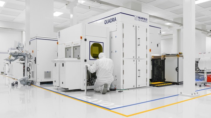
As Chips Go Vertical, Metrology Struggles to Keep Up
Semiconductor inspection has traditionally meant looking down. Optical metrology and critical dimension scanning electron microscopy (CD-SEM) systems were optimized for lateral scaling, where the central challenge was shrinking dimensions across the surface of silicon. That approach worked when transistor architectures remained relatively planar and accessible. Philippe Leray, VP of advanced patterning at imec Today, however, advanced-node manufacturing is moving increasingly into the Z-axis. Gate-all-around transistors, recessed nanosheets, HBM memory, vertically stacked NAND, hybrid bonding, and future CFET architectures are creating structures that are narrower, deeper, and more difficult to inspect. Critical variability increasingly exists along buried sidewalls and recessed regions rather than only on the top surface of the device. “Scaling is no longer happening only in the X-Y plane, but increasingly in the Z direction,” Philippe Leray, VP of advanced patterning at imec, told EE Times. “More and more, we need to look deep inside these structures to characterize defects, composition, roughness, and dimensional variation.” Traditional transmission electron microscopy (TEM) can still provide extremely detailed cross-sectional information, but it’s destructive, highly localized, and too slow for the statistical demands of angstrom-era manufacturing. Fabs increasingly need inline, non-destructive inspection methods capable of monitoring variability across production wafers in real time. That shift is driving renewed interest in techniques such as fast atomic force microscopy (AFM), scanning probe approaches, advanced X-ray systems, and hybrid metrology platforms that combine multiple inspection technologies. Why traditional metrology no longer holds upin advanced-node manufacturing Optical metrology and CD-SEM continue to play central roles in advanced-node process control, but they were largely designed for an era when critical dimensions could be measured from the top down. In advanced logic, memory, and packaging structures, important variability increasingly exists along buried sidewalls inside deep nanoscale trenches. Variations in roughness, scallops, undercuts, and etch profiles can directly affect transistor behavior, leakage, yield, and long-term reliability. According to Hamed Sadeghian, founder and CEO of Nearfield Instruments, this is becoming a growing limitation for conventional inspection techniques. “If you look at the advanced nodes, whether it’s NAND, DRAM, HBM, or logic, you have narrow deep structures,” Sadeghian told EE Times. Traditional CD-SEM systems can provide highly detailed top-down measurements, but they struggle to fully characterize buried sidewalls inside increasingly deep structures. “CD-SEMs give you a very nice top view, but not how the sidewall looks,” Sadeghian said. The challenge extends beyond logic transistors. Advanced packaging and hybrid bonding are also moving increasingly into the Z-axis, introducing additional buried interfaces and high-aspect-ratio structures that are difficult to inspect with conventional approaches. Another issue is that many conventional measurements are still performed on nearby process-control targets rather than directly on production transistors themselves. “Traditional metrology typically measures dedicated targets, markers, or structures placed in the scribe lines,” Sadeghian said. “These are not the actual device structures. They often experience different process conditions and patterning effects than the active device area, which means the measurement may not fully represent what’s happening on the device itself.” The industry’s growing reliance on TEM also illustrates the changing demands now facing semiconductor process control. TEM remains one of the semiconductor industry’s most precise tools for inspecting buried structures and sidewalls. But the technique was never designed for the statistical requirements of advanced-node manufacturing. To perform TEM analysis, wafers must be physically sliced and removed from production for cross-sectional analysis. “The wafer leaves the line,” Sadeghian said. That workflow is destructive, slow, and highly localized. Manufacturers may obtain extremely detailed information from one small region of a structure while still lacking visibility into variability elsewhere across the wafer. “We are entering the angstrom world,” Leray said. “You need statistics to reach the angstrom level of accuracy.” At advanced nodes, process control is no longer simply about measuring whether a single structure meets specifications. Manufacturers increasingly need to understand how tiny variations repeat across billions of transistors and complex 3D geometries spread across an entire wafer. That changes the role of metrology itself. Instead of relying on isolated high-precision measurements from a handful of locations, fabs increasingly need large volumes of measurement data capable of revealing process variability statistically across production. Traditional TEM can provide extremely detailed structural information, but only from small, localized regions after destructive sample preparation. That makes it difficult to scale for the statistical demands of inline manufacturing. The result is a growing push toward inline, non-destructive inspection methods capable of generating broader structural visibility during manufacturing itself. The return of AFM One consequence of these changing requirements is renewed industry interest in atomic force microscopy, capable of generating detailed structural information without destroying wafers. AFM has existed for decades and has long been valued for extremely high-resolution surface characterization. But traditional AFM systems were not originally designed for the narrow deep trenches increasingly common in advanced-node manufacturing. Now the need for statistical inspection across increasingly complex 3D structures is reviving interest in fast AFM approaches. “The idea of having statistics with AFM naturally came up,” Leray said. Several companies are now attempting to adapt scanning probe approaches to the requirements of advanced semiconductor manufacturing. Among them is Nearfield Instruments, which uses AFM-based techniques to inspect buried sidewalls inside high-aspect-ratio structures. The metrology tool vendor is collaborating with imec on process-control challenges involving CFETs, high-aspect-ratio structures, high-NA EUV, and advanced packaging. Nearfield’s approach attempts to provide TEM-like structural visibility while remaining inline and non-destructive. The company’s QUADRA platform uses an extremely small AFM probe tip to scan inside nanoscale structures. But as trenches become narrower, the probe itself must also become thinner to enter the structure. Extremely narrow probes, however, can bend under atomic interactions along the sidewall, distorting measurements and limiting accuracy. “When the tip is very narrow, even if you manage to go inside the trench, it does not give you the true structure,” Sadeghian said. Nearfield’s approach adds torsion-sensitive sensing designed to directly measure those sidewall interactions rather than treating them as measurement noise. The goal is not simply a better profile measurement, but a more complete representation of buried structures during inline manufacturing. “Instead of giving just one profile, we give a full image,” Sadeghian said, comparing the difference to seeing a single cross-section of a wall versus viewing an entire city in three dimensions. The company says the technology can inspect structures with openings as small as roughly 15 nm and aspect ratios exceeding 100 nm in depth while remaining compatible with inline semiconductor manufacturing flows. Metrology becomes a scaling bottleneck Sadeghian believes improved sidewall control could eventually influence not only manufacturing yield, but also energy efficiency in large-scale AI infrastructure. “If I control the sidewall better, I need less voltage to power that chip,” he said. “Imagine scaling this up with AI data centers and millions of these chips.” Inline non-destructive inspection could also reduce the number of wafers sacrificed for destructive analysis and lower the amount of supporting failure-analysis infrastructure required inside fabs. As semiconductor manufacturing becomes more complex, metrology itself is becoming a larger and more strategically important part of the production flow. “The number of metrology and inspection steps in a flow is increasing,” Leray said. “And proportionally, the metrology and inspection are increasing more.” Neither imec nor Nearfield believes a single inspection technology will solve every future process-control challenge. Instead, the industry increasingly appears to be moving toward combinations of optical, e-beam, X-ray, AFM, and data-analysis systems working together to create more complete visibility inside advanced semiconductor structures. For Leray, the semiconductor industry’s largest unresolved challenge is the ability to fully see what manufacturers are building inside increasingly opaque 3D devices. And that challenge, he added, is only becoming harder. “Because it’s deep. It’s opaque. And what we need to detect is small.”