Industry News
The latest news on the semiconductor and electronic-parts industry .

The Stratosphere Race: HAPS Move from Experiment to Commercial Reality
While autonomous flight is often associated with drones, a revolution in autonomy is unfolding in the stratosphere. At altitudes of about 20 km, high-altitude platform stations (HAPS) from the likes of Airbus subsidiary Aalto, Thales, and BAE Systems’ Prismatic are targeting the largely untapped airspace between most air traffic and low-Earth-orbit (LEO) satellites. Far above the clouds and high winds, these aircraft draw on solar power to stay aloft with the promise of providing persistent connectivity, Earth observation, and surveillance across vast regions below for days, weeks, and even months. In late 2024, Prismatic demonstrated that promise with its Phasa-35 high-altitude pseudo-satellite. Launched from New Mexico, the aircraft climbed beyond 20 km (66,000 feet) into the stratosphere and sustained flight for 24 hours before landing again. Two days later, it was back in the air, showcasing a rapid turnaround. The HAPS momentum continued in early 2025, when Kea Aerospace’s Atmos Mk1b set off from South Island, New Zealand, to reach over 17 km (56,000 feet) and fly for 8 hours and 20 minutes. Then, in May 2025, Aalto also pushed HAPS flight further with the launch of Zephyr from Kenya. Flying above 18 km (60,000 feet), the platform maintained a direct wireless connection to a 4G device on the ground for multiple days before heading toward Australia—crossing the turbulent Intertropical Convergence Zone twice. In total, Zephyr spent a remarkable 67 days in the stratosphere. One year on, it is getting ready for commercial applications. As Aalto COO Pierre-Antoine Aubourg noted, “We will soon extend our 67-day flight to 90 days, and [after that,] we are targeting 200 days. … Persistent stratospheric missions and capabilities are a reality.” Zephyr outside a hangar: Aalto has a purpose-built HAPS facility in Laikipia County, Kenya. (Source: Aalto HAPS) Staying power Zephyr’s ability to remain in the thin air of the stratosphere for 67 days is largely down to its extremely light, composite airframe; high-end solar cells; and lightweight, ultra-high-energy-density batteries. Weighing only 75 kg with a 25-meter wingspan, the aircraft uses InGaAs triple-junction solar cells from U.K.-based Microlink Devices to recharge its batteries, which are state-of-the-art lithium-ion cells with silicon anodes manufactured by U.S.-based Amprius Technologies. “We can capture enough solar energy during the day to charge the battery, which then has the capacity to power the aircraft throughout the night,” Aubourg said. While the HAPS operates autonomously in the stratosphere, Aalto has developed advanced flight-control software to support the aircraft during takeoff and landing. “The flight control laws take advantage of the aircraft’s flexible structure and stabilize it during dynamic weather conditions, such as vortex turbulence, making the transition between the ground and stratosphere a bit smoother,” he said. “This is a delicate [place], and we don’t want to stay in it for too long.” Zephyr shortly after takeoff: Aalto describes the aircraft as “the world’s most advanced fixed-wing aircraft.” (Source: Aalto HAPS) A key application for Aalto is secure communications relay in disaster-prone and remote regions, where Zephyr’s persistent coverage can support rapid network recovery. Back in June 2024, Japanese communications companies Space Compass and NTT Docomo invested $100 million into the company to commercialize both connectivity and Earth-observation services across Japan and wider Asia. “Japan suffers from regular earthquakes and tsunamis, so our partners want to make sure they can recover networks quickly after a disaster to limit business disruptions,” Aubourg said. Aalto has also inked deals with Indonesian communications companies Telkomsel and Mitradel to explore wireless connectivity in underserved regions of the country. And in February this year, the company launched a call to the industry to collaborate on payloads up to 8 kg for deployment in Australia’s northern region. “Around half the people in the world are lacking connectivity, and there’s a real appetite to connect locations where a ground network is not profitable,” Aubourg said. “On flat terrain, we can provide connectivity to the equivalent of 250 ground towers. So we’re now preparing for commercialization and ramping production to deliver services.” According to Aalto, such a service will provide low, 5- to 10-ms latency with direct-to-device communications via standard smartphones. But the company’s future isn’t just connectivity. Zephyr is also positioned to deliver Earth observation, promising high-resolution, low-latency, real-time imagery, video, and geospatial data to sub-20-cm resolution, bridging the gap between satellite and drones. Defense applications are also emerging, with Aalto targeting intelligence, surveillance, and reconnaissance operations. Potential services may include synthetic-aperture radar, VHF-SHF for communications interceptions, and C-X band for radar detection. “If you asked me a few years ago, I would have said connectivity was our key driver, but given today’s geopolitical situation, we are seeing interest ramping from [defense],” Aubourg said. “The military is interested in bringing connectivity directly to the soldier on the battlefield. In Ukraine, for example, this could be used to control a small fleet of low-altitude drones to attack.” U.K. final assembly line: Zephyr can provide direct-to-device connectivity, military intelligence, and Earth observation. (Source: Aalto HAPS) A different approach What connects Aalto, Prismatic, Kea Aerospace, and numerous other HAPS players is a shared focus on remarkably lightweight, fixed-wing aircraft. However, U.S. aerospace company Sceye is taking a different approach, developing a lightweight, helium-filled, fabric airship: SE2. In April this year, the autonomous platform flew for 12 days straight in the stratosphere. Traveling from New Mexico to the coast of Brazil, it held its position and altitude for more than 88 hours over several selected areas, operating continuously throughout the days and nights before completing a planned and controlled flight termination. Sceye was founded in 2014 by Mikkel Vestergaard Frandsen. (Source: Sceye) “The plan was to clock some hours while station-keeping our position off the coast of Brazil—we did that—and this has been a defining step toward unlocking the stratosphere as a new layer of infrastructure,” Mikkel Vestergaard Frandsen, founder and CEO of Sceye, said. “We see this flight as the completion of our endurance test, and that essentially means that the training wheels are now off, and our platform is ready to service clients.” Like its fixed-wing counterparts, SE2 uses solar cells—in this case, thin-film arrays—to generate its power during daylight, charging its high-energy-density lithium-sulfur batteries for nighttime operation. On-board electronics and sensors track platform status, enabling autonomous operation and controlling power and gas pressure during a day-night cycle. “We use gas to keep us up, solar power during the day, and batteries at night, feeding an electric propeller to point us into the wind,” Frandsen said. “Combined with our aerodynamic shape, this holds our position and altitude over the area of operation.” Following the success of its endurance trial, and in a similar vein to Aalto, Sceye’s next step is to test wireless connectivity in underserved regions. The company’s HAPS is now scheduled to take its first commercial test flight with its investor, Japanese telecoms and IT operator SoftBank. On this flight, the airship will transit from New Mexico to Japan, where Sceye will backhaul into SoftBank’s core network and run several connectivity demonstrations during emergency and disaster-response scenarios. For the test flight, Sceye had custom-built a stratospheric telecoms antenna, SceyeCell, designed to bring high connectivity at scale—covering the equivalent of 500 ground towers—for long durations from the stratosphere. As Alfredo Serano, Sceye’s director of EMEA, who specializes in telecoms, noted, “It’s a fully regenerative 4G or 5G node that is acting as a tower in the sky. “We spoke with different operators across different geographies and economic environments and concluded that we needed a MIMO antenna designed to balance the best possible coverage and capacity,” he added. “[The antenna] can cover between 70 and 90 km in radius—although we have demonstrated it can reach up to a 140-km radius—and can deliver a capacity north of 3.5 Gbps.” The antenna has electronic beam-steering to control the beam angle and uses motion-compensation algorithms that work with GPS location and altitude to ensure the beams are always aligned and pointing in the right direction. “We can also use mechanisms such as null-forming to avoid propagating radio-transmission signals into areas that are already covered,” Serano said. “This way, we can avoid interference with the ground towers.” Following the Japan test flight, a second platform will then move to Peru, followed by a yet-to-be-named location for its second and third test flights, which will all take less than a year. And from here, Frandsen is confident that mass-market connectivity will follow, which is his company’s main focus over the emerging defense markets that fixed-wing aircraft are edging toward. “Mass-market connectivity requires us to fly this 250-kg antenna with between a 4- and 5-kW power draw to the payload,” he said. “In contrast, fixed-wing operators [typically] fly around five kilos to the stratosphere.” According to Frandsen, initial operations in Japan could involve a fleet of HAPS “parked” over the country that can then converge on the region that’s been struck by disaster, be it a tsunami, earthquake, or typhoon. He is also certain the tech can work alongside LEO satellites and small satellite constellations, as well as ground networks, to form a ubiquitous network that serves everyone. “I believe that all the real-time services from, say, autonomous vehicles, that are the promised land of 6G, are highly likely to take place in the stratosphere,” he said. “So let’s have all three layers talking together: traditional telcos with stratospheric infrastructure with LEO constellations.” As Sceye readies for Japan and Aalto explores Indonesia, other HAPS players are looking to roll out services from the stratosphere. Industry sources indicate that NASA, on behalf of the Air Force Research Laboratory, has awarded a $10 million contract to Prismatic to deploy airborne surveillance missions. Meanwhile, Kea Aerospace is preparing flights around New Zealand to monitor water quality as well as missions over Antarctica to track ozone levels. And away from mass connectivity, Sceye has identified methane leaks over the Permian Basin in New Mexico. “Going forward, I do think that the biggest role we have is a normative one,” Frandsen said. “We want to make HAPS normal.” Read also: Mikros Technologies and Carbice Corporation are adapting technology originally created for the International Space Station to solve heat-dissipation problems in AI data centers.

Gartner Says Supply Chain Confronts Geopolitical and AI Challenges
Gartner’s Santalo highlights strategies to navigate chaos, orchestrate agility, and accelerate Innovation. BARCELONA, Spain — During last week’s Gartner Supply Chain Symposium/Xpo, Alejandro Santalo, a senior director analyst at Gartner, outlined in an interview with EE Times the primary challenges and strategic adjustments that chief supply chain officers face today. Santalo argued that executives must adapt operational models to address capacity constraints driven by data center growth and new import restrictions in a complex global market. Image by Valerii Iavtushenko from Pixabay Geopolitics and regulatory pressures The regulatory environment governing technology imports is tightening, signaling a broader movement toward supply chain decoupling. The recent May 2026 summit between the U.S. and China highlighted an acceleration toward what analysts term “corporate geopolitics.” According to Santalo, this concept involves using corporate capital, industrial ecosystems, and private-sector speed as instruments of geopolitical influence and economic strategy. Traditional diplomacy relies on slow regulatory reviews and long implementation cycles, but corporate action compresses this timeline through private-sector execution speed. Santalo advised executives “should prepare for rapid shifts in sourcing, industrial investment, energy competition, and manufacturing alignment as the May 2026 Trump-Xi summit highlighted a shift toward corporate geopolitics.” Alejandro Santalo (Source: Gartner) Specifically, he recommended that leaders assess alternative supply partners, evaluate capital allocations, monitor policy developments, and build operational flexibility. He noted that CEOs, capital markets, and industrial policy will reshape supply chains faster than traditional diplomacy. This geopolitical tension is increasingly manifesting in targeted regulatory actions, such as the U.S. Federal Communications Commission’s decision to ban consumer routers manufactured abroad. Santalo views this development as an early signal for broader network decoupling, warning that the language used in the order centers on protecting national security. “While the order clearly focuses on consumer routers, supply chains must consider that similar actions could be taken in the future for other products and technologies, as it can be seen in the growth of the list of equipment and services deemed to pose an unacceptable risk to national security,” Santalo said. Organizations producing critical technologies should develop scenario-based playbooks to anticipate and address regulatory shifts. For companies impacted by restrictions, Santalo recommended seeking conditional FCC approval to keep market access while relocating production to compliant regions. Hyperscalers and capacity constraints AI is fundamentally reshaping hardware demand patterns, creating a severe capacity shortage for legacy technology buyers. The requirements of hyperscalers are redirecting semiconductor manufacturing capacity. Hyperscaler influence has reshaped demand patterns, eliminating traditional seasonality in the high-tech sector. Memory manufacturers now prioritize high-bandwidth memory for data centers, making other sectors compete for the remaining capacity. Micron’s Fab 6 in Manassas, Virginia (Source: Micron) This environment requires a shift away from standard procurement strategies focused primarily on price negotiations. “You need to work long-term relationship securing capacity,” Santalo explained, adding that for supply chain leaders, “it’s not about margin, it’s about protecting revenue.” Ensuring that capacity is available is the only way to capture revenue when competitors face supply shortages. With hyperscalers reportedly placing capacity orders for 2028 and 2030, companies attempting to negotiate allocations for 2026 are already arriving too late to the market. The complexity of semiconductor manufacturing compounds the issue, as companies cannot easily shift production lines or find alternative fabrication facilities for advanced processing nodes. Advanced semiconductor manufacturing remains highly concentrated in Taiwan, and Santalo recommended supply enablement over disruption avoidance to secure supplier access and market share. AI integration strategies On the operational side of AI, Santalo noted a widening maturity gap between leading supply chain organizations and the rest of the industry. The most advanced companies distinguish themselves through a disciplined approach to technology adoption. First, they focus heavily on data readiness, ensuring that previously siloed information is accessible to decision-makers in real time. Second, they deploy AI to address specific business challenges rather than adopting the technology for its own sake. As Santalo advised clients, “Do not create an AI strategy, infuse your strategy with AI.” These mature companies are also redesigning their processes to accommodate AI, expecting that autonomous agents will soon run many workflows independently, with human involvement focused primarily on oversight, governance, and exception management. Santalo noted that companies such as Microsoft have publicly committed to deploying hundreds of agents to run supply chain operations. Furthermore, leading firms extend their AI integration beyond their internal operations, connecting their ecosystems with external partners to gain visibility into lower-tier suppliers. Despite the rapid adoption of new technologies, Santalo identified significant operational missteps across the sector. One common error is the singular focus on generative tools at the expense of established analytics. “Many companies are ignoring traditional AI and machine learning because of the hype of generative AI,” Santalo noted, emphasizing that traditional machine learning remains highly effective. Santalo warned that deploying agentic AI can introduce new vulnerabilities. He recommended that organizations update operating models and governance frameworks to mitigate cyber, operational, and compliance risks and to prevent supply chain disruptions. Diversification and circular economy In response to geopolitical risks and supply constraints, high-tech manufacturers accelerate the geographic diversification of their production networks. Santalo shared industry data indicating a clear intention among electronics companies to increase manufacturing capacity in countries such as Vietnam, India, Mexico, and the U.S. He described this realignment as an “insurance policy” for companies seeking to protect their most critical revenue streams against potential policy changes or tariff implementations. However, this shift creates new complexities, as modern PCBs contain thousands of components that must navigate a complicated matrix of export controls and local regulations. Simultaneously, the concept of circularity within the electronics supply chain is evolving from an environmental mandate into a practical sourcing strategy. Santalo noted a distinct shift in corporate mindset, where companies view the reverse supply chain as a new source of supply for scarce materials. Rather than merely refurbishing entire products, specialized recycling firms are increasingly focused on salvaging viable components directly from hardware or recovering raw metals through industrial smelting. Santalo recommended that supply chains prioritize reverse-supply items based on their value to resilience, with a particular focus on scarce materials, volatile commodities, and critical components. By collaborating with regional partners on localized recycling or energy projects, companies can stabilize their supply lines and reduce overall risk in an increasingly constrained global market.

Qilimanjaro Pushes Analog Quantum as AI Compute Demands Surge
Most quantum computing companies are pursuing gate-based digital quantum systems. These machines manipulate qubits through long sequences of quantum logic gates, similar in concept to how conventional processors execute instructions. But every interaction with a qubit risks introducing noise and decoherence, forcing digital systems to rely heavily on error correction and large numbers of redundant physical qubits. A small group of quantum computing companies is pursuing an alternative architecture known as analog quantum computing, arguing that it may reach useful applications sooner than many gate-based quantum systems. Among them is Qilimanjaro Quantum Tech, a Barcelona-based startup. “We believe in this vision of multimodality,” Marta Estarellas, CEO of Qilimanjaro, told EE Times. “If you have a problem that is intrinsically continuous, like chemistry or electrodynamics in materials, analog is more suitable. If you have a more structured mathematical problem, such as in cryptography, use a digital approach.” Qilimanjaro is one of the few firms pursuing analog quantum computing. According to Olivier Ezratty, a quantum computing academic and co-founder of the Quantum Energy Initiative, other companies in this category include D-Wave, Pasqal, and QuEra. Reducing the gate problem Qilimanjaro’s central argument is that analog quantum systems may be able to reduce the accumulation of errors by avoiding many of the gate operations required in digital quantum computing. “There’s indeed no such thing as gate operations in quantum annealing and analog quantum simulation,” Ezratty told EE Times. In digital quantum computers, each gate operation requires interacting with fragile qubits using fast microwave pulses or other control mechanisms. Those interactions can disturb the system and create errors that compound throughout a computation. Qilimanjaro instead uses analog quantum evolution. Rather than repeatedly manipulating qubits through discrete gate sequences, the system prepares a quantum state and allows it to evolve more naturally toward a minimum-energy solution. “You prepare your quantum chip, and you let it go,” Victor Canivell, chairman and co-founder of Qilimanjaro, said. “Because you don’t interact with it all the time, you create far fewer errors.” The company uses superconducting qubits—similar to those used by IBM and Google—but of a slightly different type, the fluxonium qubit, which allows for analog control on top of digital. Qilimanjaro believes this could make analog systems particularly useful for problems involving continuous physical processes, including chemistry, materials science, optimization, and, potentially, AI training. Industrial companies are already exploring some of those use cases. Repsol, a Spanish multinational energy company headquartered in Madrid, sees analog quantum systems as potentially useful for large-scale optimization and energy system design. The company is now working with Qilimanjaro to find out more. “At Repsol, we are increasingly facing industrial challenges where complexity grows faster than compute, particularly in optimization problems,” Emilia Martínez, CTO of Repsol, told EE Times. “Quantum computing offers a fundamentally different way to explore these complex solution spaces.” AI becomes a new target Although quantum computing has long been associated with chemistry simulation and optimization, Qilimanjaro increasingly sees AI as one of the most promising future applications for analog quantum systems. The transition comes as hyperscalers and AI companies confront growing power consumption challenges associated with large-scale AI training and inference. “We are seeing now a huge interest in quantum computing that we never saw before,” Estarellas said. “The digital world is realizing that we need a more sustainable way of doing computation.” Qilimanjaro believes analog quantum systems could eventually become specialized accelerators inside future AI infrastructure. The company is particularly focused on “quantum reservoir” approaches to AI training. These systems use the complex dynamics of quantum systems themselves as computational resources for machine-learning tasks, particularly for the prediction of time series. According to Estarellas, recent theoretical papers from outside research groups have strengthened interest in the concept. “This can become the biggest revolution since Nvidia exploded with GPUs,” she said. The company argues that quantum systems may eventually support larger and more complex neural networks than classical systems can efficiently simulate. “As the quantum systems grow bigger and bigger, the complexity of the neural network that we can encode grows exponentially with the number of qubits,” Estarellas said. Still, Qilimanjaro acknowledges that practical quantum advantage in AI remains unproven. “We still need to run those algorithms on real quantum hardware, and that is why we are building our next-gen chips,” Estarellas said. Ezratty also cautioned that proving meaningful quantum advantage remains difficult across the analog quantum sector. Building a hybrid quantum infrastructure Qilimanjaro positions its systems not as standalone replacements for classical computing but as components within future hybrid infrastructures that combine HPC, AI accelerators, and multiple types of quantum hardware. The company has deployed systems at the Barcelona Supercomputing Center (BSC), where researchers are experimenting with hybrid HPC-quantum workflows. According to BSC senior researcher Alba Cervera-Lierta, the center is integrating both analog and digital quantum systems into a dedicated partition of the MareNostrum 5 supercomputer called “MareNostrum ONA.” Researchers are exploring approaches that distribute workloads across classical HPC systems and quantum computers. Cervera-Lierta also noted that quantum simulation is already emerging as a promising application area for hybrid HPC-quantum systems because some physics simulations stretch beyond the capabilities of classical supercomputers. Qilimanjaro sees such deployments as early models for future data centers. “The future of the data center will be traditional computing, AI computing, and quantum computing together,” Canivell said. Barcelona Supercomputing Center’s Alba Cervera-Lierta standing under the first quantum computer in Spain, developed with 100% European technology. The quantum computer is integrated with the MareNostrum 5 supercomputer at BSC. (Source: Mario Ejarque/Barcelona Supercomputing Center) Scaling challenges remain Despite the optimism surrounding analog quantum systems, major technical challenges remain. Qilimanjaro currently operates prototypes with 15 analog qubits and is developing systems with roughly 50 analog qubits. The company believes that useful “quantum utility” or business advantage in specific applications could emerge within two to five years. “I think this will happen within a range of two to five years, probably in the lower range,” Estarellas said. Quantum Energy Initiative’s Olivier Ezratty (Source: Franck Disegni) But commercial-scale systems remain far more difficult. Superconducting quantum systems require extreme cryogenic cooling, sophisticated control electronics, and dense cabling infrastructure. Scaling those systems introduces fabrication, packaging, and noise challenges. “The fabrication process is still very artisanal,” Estarellas said. “You make human mistakes. The yield of those devices is not always very good, and we must start automating those processes.” Cervera-Lierta also pointed to broader industry hurdles surrounding fault tolerance and scaling. She said large-scale practical quantum computing may eventually require networking multiple quantum systems together because future machines may not fit within a single dilution refrigerator. Ezratty added that analog quantum systems face their own scaling limits, particularly around coherence time and the physical behavior of large quantum systems. Even so, Qilimanjaro argues that analog quantum systems may provide a nearer-term route to practical applications than fully fault-tolerant, gate-based quantum computers. The company said it deliberately positions itself against some of the hype surrounding quantum computing. “We decided to follow the anti-hype approach,” Estarellas said. “Every claim, every presentation we made, was based on scientific grounds.” That strategy may help the company stand out as the quantum industry increasingly shifts attention from long-term theoretical potential toward practical utility, infrastructure integration, and AI-era computing demands. Read also:

Majestic Labs Raises $100M for Memory Pooling AI Server
Server architecture will offer up to 100 TB of DRAM per accelerator. LOS ALTOS, Calif. — AI chip startup Majestic Labs is working on a memory-pooled server design for AI inference that will offer as much as 100 TB of DRAM per accelerator, far beyond what can be achieved with HBM today. The company has raised $100 million in Series A funding for its chip and system design, which can pack the memory capacity and bandwidth of 10 racks of state-of-the-art GPUs into a single server, Majestic Labs co-founder and president Sha Rabii told EE Times. Majestic Labs was founded in 2023 by longtime colleagues Masumi Reynders, Ofer Shacham, and Sha Rabii after a long history of working together in the silicon divisions of Google and, more recently, Meta. “We spent a lot of time thinking about the opportunities—not just where AI is today, but extrapolating, looking at where it was, where it is, where it’s likely to be, and trying to shoot ahead,” Rabii said. “Because we knew from the get-go that it was foolish to try and play Nvidia’s game and just out-execute them.” From left to right: Majestic Labs co-founders Sha Rabii, Ofer Shacham, and Masumi Reynders (Source: Majestic Labs) The founders’ observation was that compute was growing faster than memory bandwidth, while the inference of most large models was memory bandwidth-limited. They anticipated that models would continue to grow in size and that longer context lengths would be required, Rabii said. “[We knew] people would want the quality of results you get from top-of-the-line models, but the economics would be very challenging,” he said. The economics of compute-first architectures—starting with a highly performant compute element and fitting as much HBM as possible around it—are based on sub-optimal compute-to-memory ratios, Rabii said. “We decided to come up with a technology that disaggregates memory from compute, so you can scale memory independently of compute,” he said. “The big challenge is connecting the memory and compute through an extremely high bandwidth and low latency interface that can compete with HBM.” HBM connects a relatively small amount of memory to compute at high bandwidth, and CXL can connect large memories with low bandwidth, but neither fully meets the requirements of AI, Rabii said. Majestic’s memory-first architecture tackles the issue with memory pooling. Since this requires extremely high-bandwidth I/O, the team started working on ways to implement the physical layer, protocols, and software layer immediately, as well as considering how to manage reliability and robustness against failures. Two dies Majestic is working on two pieces of silicon—a memory interface chiplet which will sit next to both compute and memory, and a many-core AI acceleration chip. Majestic’s memory pool design uses over 100 TB of standard LPDDR in a server alongside up to 12 of Majestic’s AI accelerator chips. The memory pool will use loose coherency with proprietary mechanisms for flow control and atomic operations, and striping schemes will be used to fully utilize the available bandwidth. The entire memory space is accessed by an AI compute chip as a single contiguous flat memory space, with each compute chip having the same bandwidth and latency to every location in that memory space. “That really simplifies programming,” Rabii said. GPU-based servers tend to have many tiers of memories (local HBM, HBM on other GPUs, host LPDDR, etc.), which makes optimizing performance a complex software task. “There are entire companies whose reason for existence is to help other companies map their workloads more effectively and efficiently to GPU clusters,” Rabii said. “We think that is an unnecessary task… [we need to] build the infrastructure in a way that is usable.” Developers don’t want to have to learn anything about how hardware works, Rabii said, though they inadvertently carry implicit assumptions about how compute and memory operate to their coding. For this reason, Majestic wants to try to maintain a compute and memory mindset, rather than going with a novel accelerator design. Majestic’s accelerator is fully programmable with a large array of CPU cores and matrix multiplication accelerators. The startup has licensed accelerator IP from a third party, which is building a custom version of its core for Majestic’s accelerator. Crucially, this third party is also able to supply the compiler and low-level software for its IP.Since AI workloads are not compute-bound, Rabii said, the accelerator design is less critical than the memory interface and system architecture. “It isn’t really about the hardware—the success of servers has as much to do with how quickly people can ramp up and use them and how robust your toolchain is, as how close it gets to the limits of [performance],” Rabii said. “I have Google and Meta to thank for really making me internalize that.” Today, Majestic’s software stack can take HuggingFace models and lower them to executable code that can run on a software simulation of its server. The company is leaning toward open-source software projects such as Triton and vLLM, Rabii said. High bandwidth The success of Majestic’s server will depend on the bandwidth it can achieve between its accelerators and off-package DRAM. The actual memory in HBM is the same as what’s in LPDDR, Rabii pointed out, but HBM gets the bandwidth by stacking lots of memory dies and aggregating their bandwidths through a proprietary interface. “We do something analogous to that but on a different scale,” he said. “We take groups of LPDDR chips, aggregate their bandwidths, and connect them through a proprietary very high-speed interface to our compute chips.” The LPDDR is mounted on boards using off-the-shelf technology, Rabii said, in order to bring the server to market quickly. Not using HBM helps both economics and the supply chain for Majestic, he added. Flexibility One of the key advantages of Majestic’s architecture is that it can offer flexible compute-to-memory ratios. The Majestic server can be equipped with between one and 12 compute chips, and memory can scale from 8 to 128 TB. More compute cards can be added after deployment to change the ratio, Rabii said. “If you wanted to build a data center out of entirely Majestic servers, you could configure some for prefill with high compute and modest memory, and do the converse for decode,” he said. “But we’re agnostic—if a customer wants to use Nvidia for prefill and Majestic for decode, [they can].” Target customers include hyperscalers, neoclouds, and large enterprises, especially those in high-frequency trading. The company already has had multiple customers place significant orders for its servers, Rabii said. “Everyone, whether they admit it or not, is focused on the cost of running AI models,” he said. “That’s where we have a significant advantage.” Today’s GPU-based systems often over-specify the number of GPUs purely to increase the amount of memory available, which results in low GPU utilization. “This would mean buying a lot of very expensive silicon you don’t really need, which also uses a lot more power,” he said. “One of our servers supports many more users than a GPU server; that’s a big cost advantage.” The company currently has a team of 40 split between Los Altos, Calif., and Tel Aviv, Israel. Both Majestic’s AI compute chip and its memory interface chiplet will tape out this year. Servers will begin shipping to lead customers in 2027. Read also: Delos Data wants to enable practical scale-up domains of 1000+ GPUs in flexible topology designs. RELATED TOPICS:AI, AI ACCELERATOR, AI INFERENCE, DATA CENTERS, MEMORY, MEMORY POOLING, SEMICONDUCTORS, STARTUPS COMPANIES:MAJESTIC LABS _Sally Ward-Foxton covers AI for EETimes.com and EETimes Europe magazine. Sally has spent the last 18 years writing about the electronics industry from London. She has written for Electronic Design, ECN, Electronic Specifier: Design, Components in Electronics, and many more news publications. She holds a Masters' degree in Electrical and Electronic Engineering from the University of Cambridge._Follow Sally on LinkedIn 0 comments

AI in Design Verification: From Experimentation to Measurable Capability
AI in design verification, or “AI in DV”, has moved from speculative discussion into practical engineering trials. Verification teams are already examining AI-assisted approaches for regression triage, debug support, coverage analysis, failure clustering, log summarization, and knowledge retrieval. That shift is useful, but it also changes the question. The industry is no longer only asking whether AI can help with isolated tasks. In many bounded cases, it can. The more important question is whether “AI in DV” improves measurable verification capability inside real project flows. This distinction matters because verification is not simply a productivity activity. It is a confidence-building discipline. The objective is not to produce more artefacts, tests, or reports. The objective is to reduce functional risk, close meaningful coverage gaps, preserve traceability, and support defensible signoff decisions. Industry studies continue to frame functional verification as a critical challenge as semiconductor design complexity grows [1]. That makes AI attractive, but it also means adoption must be judged by engineering outcomes rather than novelty. Local productivity is not the same as verification capability The first trap in “AI in DV” adoption is to confuse task acceleration with capability improvement. A model may summarize a regression log faster than an engineer. A classification engine may group failures more quickly. A retrieval assistant may help engineers find methodology guidance or past debug notes. These are valuable improvements, but they are local improvements. They do not automatically prove that the verification process has become more reliable, more complete, or more predictable. Verification works as a system. Testbenches, assertions, coverage models, regression systems, issue tracking, review gates, and signoff evidence all interact. Standards such as UVM exist to support reusable, interoperable, and structured verification environments [2]. Portable stimulus reflects a similar need to express verification intent across multiple execution platforms and abstraction levels [3]. These standards highlight an important point: Mature verification is built around disciplined flow integration, not isolated tool activity. For that reason, the useful question is not, “Did AI generate an output?” It is, “Did that output improve the flow?” If AI reduces debug time but its recommendation is not reviewed, logged, or linked to a root cause, its operational value is limited. If AI creates additional tests that are not connected to coverage intent, the team may increase activity without reducing risk. If a knowledge assistant provides a plausible answer but cannot point to the underlying source, engineers still need to validate the result manually. The measurement problem, therefore, becomes central. “AI in DV” has to be assessed against verification outcomes, not usage counts. AI in DV capability measurement view (Source: author’s analysis) The figure shows how “AI in DV” adoption can be assessed across practical capability dimensions, including data readiness, workflow integration, governance, pilot measurement, skills, and scalability. The chart is intended as an illustrative view of capability improvement. The operational risk of tool-first adoption A second common problem is tool-first adoption. A team sees a promising model, a vendor demonstration, or an internal prototype, then looks for a place to use it. This approach can create visible experimentation, but it often produces weak operational learning. The symptoms are familiar. One group experiments with log summarization. Another builds a script for failure grouping. A third tries AI-generated tests. A fourth creates a chat interface for methodology documents. Each pilot may produce something useful, but the organization still lacks a clear view of where AI improves capability, which data can be used safely, who reviews outputs, and how the results fit into the existing flow. This is not just a process concern. It is an engineering control concern. Regression and debug automation already demonstrate the value of structured management, as failing tests can be sorted, triaged, and categorized by root cause and linked back to verification planning [4]. AI can extend these capabilities, but only when the surrounding workflow remains controlled. Without that control, teams can accumulate AI-generated artefacts that are hard to reproduce, audit, and trust. A summary may be helpful but incomplete. A failure cluster may group unrelated issues. A generated test may exercise behavior without proving that it targets an intended scenario. These risks are manageable, but only if the adoption model is designed around review, traceability, and operational measurement from the start. What should be measured? The most important “AI in DV” metric is whether the verification organization becomes better at reducing risk within project constraints. Useful measures include regression turnaround time, debug cycle time, quality of failure clustering, reduction in duplicate failure analysis, review consistency, coverage closure efficiency, and engineer time saved on repeatable tasks. Where project data allows, teams can also examine whether AI-assisted workflows improve earlier bug discovery or reduce late-stage surprises. Coverage closure is a useful example. The challenge is not simply reaching a number. Engineers need to understand what has been covered, what remains untested, which tests contribute useful coverage, and where remaining gaps indicate real risk. Coverage planning, closure, and root cause analysis are recognized as difficult, iterative parts of SoC verification [5]. AI can help by identifying patterns in coverage data, prioritizing investigation, or suggesting areas for directed stimulus. But the measure of success is not how many suggestions were produced. The measure is whether engineers reached better closure decisions with less wasted effort and maintained confidence in the evidence. Regression triage is another practical example. Large regressions generate repeated failures, duplicate signatures, and noisy logs. AI-assisted grouping can reduce manual sorting and help teams focus on new or high-risk failures. But the metric should include classification accuracy, engineering review effort, false grouping rate, and traceability to the confirmed root cause. A faster triage process that hides uncertainty is not an improvement. Debug support follows the same logic. AI may help identify likely sources of failure, compare passing and failing runs, or point engineers to suspicious changes. Commercial EDA material already shows AI being applied to debug productivity, regression turnaround, and test failure classification [6]. The operational question is whether these capabilities shorten the debug loop while preserving engineering accountability. Where AI can help, and where caution is needed The most suitable near-term uses of “AI in DV” are bounded, repetitive, and reviewable. Regression triage, log summarization, failure clustering, coverage gap analysis, documentation search, and review assistance fit this pattern. They generate data, have recurring workflows, and leave space for human judgment. This is particularly relevant in debug-intensive verification environments, where engineering effort is often concentrated in analyzing failures, isolating root causes, and deciding which issues require deeper investigation. Where verification effort is concentrated. (Source: Wilson Research Group Functional Verification Study, published by Verification Horizons / Siemens EDA) The Wilson Research Group Functional Verification Study shows that debugging remains one of the largest time consumers for IC/ASIC verification engineers. This supports the case for measuring “AI in DV” through operational outcomes such as debug cycle time, triage quality, repeated failure analysis, and review consistency, rather than by the number of AI-generated outputs alone. The risk increases when AI moves closer to interpreting intent or influencing signoff. Automated interpretation of ambiguous specifications is difficult because specifications often contain assumptions, exceptions, and architectural context that are not fully machine-readable. Unsupervised test generation can also create problems if generated tests are not linked to verification intent, coverage goals, or review criteria. More activity does not necessarily mean better verification. The highest-risk area is AI involvement in signoff decisions without traceability. Verification signoff depends on evidence. If an AI recommendation cannot be reproduced, reviewed, or connected to source data, it should not be treated as signoff evidence. AI may support the process, but it cannot become an unexamined authority within it. Governance is part of engineering, not administration Governance is sometimes treated as a brake on innovation. In verification, it is better understood as part of the engineering discipline. AI outputs that influence verification work should be logged, reviewable, and linked to the inputs that produced them. Teams need to know which data was used, which model or configuration produced the output, who reviewed it, and how the decision was accepted or rejected. These requirements become more important as AI moves from convenience functions toward workflow decisions. AI governance as a foundation for measurable adoption (Source: NIST, “AI Risk Management Framework.” Credit: N. Hanacek/NIST) The NIST AI Risk Management Framework defines Govern, Map, Measure, and Manage as core functions for managing AI risk. In “AI in DV”, the same discipline applies when AI-assisted outputs influence regression triage, debug support, coverage interpretation, or signoff evidence [8]. For verification teams, the implication is clear: AI adoption should include risk controls, not only productivity expectations. This is especially important where sensitive design data is involved. RTL, verification plans, coverage databases, logs, specifications, and bug histories are valuable IP. “AI in DV” adoption must therefore address data access, model deployment, retention policies, and auditability. These are not separate from engineering success. They determine whether AI can be used safely at scale. From experimentation to measurable capability The next phase of “AI in DV” should start with a narrower question than many teams ask today. Instead of asking, “Where can we use AI?”, the more useful question is, “Which verification capability do we need to improve, and how will we measure it?” That question leads to better pilots. A strong pilot has a defined workflow, a baseline metric, a controlled dataset, a review process, a failure mode, and a scaling condition. It does not try to transform verification in one step. It demonstrates whether AI improves a single meaningful part of the flow without weakening traceability or accountability. This is also where operational management becomes important. Engineering leaders need to compare opportunities, select measurable use cases, and decide when a pilot is ready to scale. The practical value of “AI in DV” will come from repeatable improvements that can be integrated into the verification organization and trusted by the engineers responsible for signoff. The next phase of “AI in DV” will not be defined by who experiments first, but by who can measure, govern, and scale it inside real verification flows. References: 1] H. Foster, “[2024 Siemens EDA and Wilson Research Group Functional Verification Study: 7-Part Video Series,” Verification Academy, Feb. 17, 2025 2] Accellera Systems Initiative, “[Universal Verification Methodology (UVM),” Accellera 3] Accellera Systems Initiative, “[Portable Test and Stimulus Standard,” Accellera 4] B. Bailey, “[AI-Driven Verification Regression Management,” Semiconductor Engineering, Apr. 24, 2025. Read also:
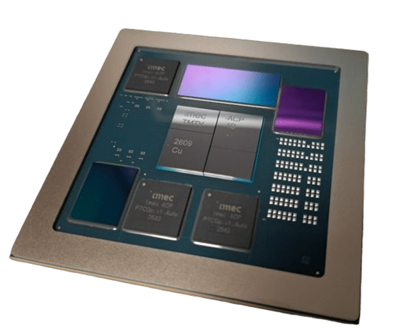
Chiplets, Ecosystems, and Europe’s Post-Fab Semiconductor Strategy
For years, Europe’s semiconductor ambitions were measured in fabs, process nodes, and manufacturing sovereignty. The European Chips Act elevated semiconductors to the level of strategic industrial policy, triggering a wave of subsidies and investment proposals aimed at rebuilding manufacturing capacity across the continent. Yet despite those efforts, Europe’s position in the global semiconductor industry continues to weaken. Few executives have watched Europe’s semiconductor industry evolve as closely as Maria Marced, who now helps shape discussions around Chips Act 2.0. According to Marced, Europe’s global semiconductor market share could fall to around 6% this year. Maria Marced “That’s quite pathetic, frankly speaking,” Marced told EE Times. “The focus now on the Chips Act 2.0 is the other way around. The focus is more on [the] end-to-end ecosystem, from chips up to the final product.” That shift reflects a broader transformation underway across the semiconductor industry itself. As AI, autonomous systems, robotics, and advanced edge computing drive exponentially greater compute demands, semiconductor architectures are becoming increasingly modular and heterogeneous. Instead of relying exclusively on ever-larger monolithic chips, companies are increasingly assembling systems from multiple interconnected components—chiplets—linked through advanced packaging and high-speed interfaces. For Europe, that transition may create an opportunity to compete differently. Rather than attempting to replicate the manufacturing scale of Taiwan, South Korea, or the U.S., Europe is increasingly positioning itself around what some industry leaders see as the semiconductor industry’s next strategic layer: ecosystem coordination, interoperability, advanced packaging, and system-level integration. Automotive pushed imec toward chiplets Imec’s Peter Vandersteegen At imec, Peter Vandersteegen, portfolio manager for automotive, is helping lead the organization’s transition from its Automotive Chiplet Program toward a broader Autonomous Edge Chiplet Program spanning robotics, security, and AI-driven systems. The shift began with automotive. “The high-performance compute is basically determining your relation with the car,” Vandersteegen told EE Times. “But to make that happen, you actually need a large amount of compute power in that car.” The challenge, however, is economic as much as technical. Autonomous driving systems increasingly require leading-edge semiconductor technology, but automotive volumes remain relatively limited compared with hyperscale AI or smartphone markets. Developing fully custom monolithic processors at advanced nodes is becoming prohibitively expensive for many automotive applications. “To develop a high-performance compute engine, you actually need scale to justify that investment,” Vandersteegen said. “However, those technology nodes, especially the development, are quite costly. And the amount of cars is not increasing.” That pressure is helping drive interest in chiplets—modular semiconductor building blocks that can be integrated into larger systems through advanced packaging technologies. Rather than designing an entirely new chip for every application, companies can reuse and combine smaller functional blocks across multiple systems and industries. “Chiplets simply are a way to support high-performance compute because they basically enable scalability and modularity,” Vandersteegen said. What began as a solution to automotive compute economics quickly evolved into something larger. Imec realized that many of the same requirements shaping autonomous vehicles also apply to robotics, industrial automation, and other AI-driven autonomous systems. Those systems must interact safely with unpredictable environments, while balancing increasingly complex compute demands against limited deployment volumes—limited at least in the initial phases. As a result, imec’s focus gradually expanded from automotive-specific chiplets toward broader ecosystem infrastructure. The rise of interoperability ecosystems That transition also exposed one of the central realities of heterogeneous integration: Chiplets only work at scale if components from multiple vendors can interoperate reliably. Vandersteegen said global standards will help overcome that challenge. The shift toward chiplets changes more than chip architecture. It changes the structure of the semiconductor industry itself. Instead of vertically integrated systems built largely within a single company, heterogeneous integration increasingly depends on coordination across foundries, chip designers, packaging specialists, software developers, automotive suppliers, and standards committees. That reality is pushing organizations such as imec into areas that historically sat outside traditional semiconductor R&D. Vandersteegen said the institute’s Automotive Chiplet Program increasingly focused on issues such as reliability validation, thermal stress analysis, compliance testing, and multi-vendor interoperability. The goal is not simply to develop chiplets, but to create the infrastructure necessary for chiplet ecosystems to function reliably in demanding environments such as autonomous vehicles. To support that effort, imec established a new site in Heilbronn, Germany, focused on prototyping and compliance testing for chiplet-based systems. It is also participating in efforts to standardize chiplet interfaces, an increasingly strategic issue as heterogeneous computing systems become more modular and multi-vendor by design. In many ways, the rise of chiplets resembles earlier platform transitions in computing and telecommunications, where standards and ecosystem control often became as important as the underlying hardware itself. Europe’s post-fab opportunity Marced argues that this transition may align unusually well with Europe’s industrial structure, particularly in automotive and industrial systems. “Chiplets could be a good approach to solve all the questions around the technology in automotive,” she said. Unlike hyperscale cloud computing or consumer smartphones, automotive systems prioritize long lifecycles, safety, reliability, and integration across complex industrial supply chains— areas where Europe has historically maintained strong expertise. For Marced, Europe’s future competitiveness may depend less on matching Asia’s manufacturing scale and more on building end-to-end ecosystems around design, integration, and heterogeneous computing. “Instead of building fabs, it’s about focusing on design,” she said. That doesn’t mean fabs become irrelevant. Europe continues to pursue manufacturing investments through projects involving Intel, TSMC, STMicroelectronics, and GlobalFoundries. But industry leaders increasingly acknowledge that manufacturing scale alone is unlikely to restore Europe’s semiconductor leadership. “Can Europe realistically compete on leading-edge fabs alone?” Marced said. “No.” Instead, Europe’s opportunity may lie in becoming indispensable in the infrastructure layer surrounding heterogeneous computing systems: advanced packaging, chiplet interoperability, automotive integration, prototyping, and ecosystem coordination. That shift is also beginning to influence discussions around Chips Act 2.0, which Marced said is increasingly moving beyond a pure manufacturing focus toward broader support for ecosystem development, startups, and design capabilities. Imec’s thermal mechanical test vehicle determines the reliability of chiplet-based systems in packages. (Source: imec) The next semiconductor battleground The broader implication is that semiconductor leadership itself may be changing definition. For decades, the industry’s center of gravity revolved around transistor density and manufacturing scale. But as heterogeneous systems become more complex, value may increasingly shift toward the ability to coordinate ecosystems spanning multiple technologies, companies, and industries. In that environment, interoperability standards, shared platforms, and integration infrastructure become strategic assets. “Whenever you lead a movement, whether it’s standards or ecosystems, being a central figure helps you win the market,” Marced said. Ironically, the collaborative and cross-border structure that has often been viewed as a weakness for Europe’s semiconductor industry may become more relevant in a chiplet-driven era where no single company can build every part of the system alone. The next semiconductor race may still involve fabs. But increasingly, it may also revolve around who defines the interfaces, standards, and ecosystems that connect them. Read also:

Vicinity Unveils “TRAVE” — AI-Native SDR Platform at 5G-ACIA Frankfurt
_Programmable AI-native 5G SDR platform combines edge AI, software-defined wireless IP, mesh networking, and future TN/NTN evolution for next-generation industrial communications_ Frankfurt, Germany — May 28, 2026 — Vicinity Technologies Limited today officially unveiled TRAVE, its next-generation AI-native 5G/6G Software Defined Radio (SDR) platform, during the 5G-ACIA 5G User Conference in Frankfurt. Designed for industrial automation, robotics, autonomous systems, private wireless infrastructure, and mission-critical communications, TRAVE represents Vicinity’s latest advancement in programmable wireless technologies and proprietary SDR intellectual property. Powered by the latest NXP Semiconductors i.MX 95 AI application processor together with the Layerscape LA9310 and LA12xx family wireless processing platforms, combined with Vicinity’s developed SDR PHY/MAC software stack, TRAVE delivers: AI-native wireless architecture Programmable 5G and future 6G SDR technologies Software-defined PHY and MAC processing Native mesh and sidelink networking Deterministic ultra-low latency communications Flexible RF integration architecture Future TN/NTN converged wireless evolution Software-upgradable industrial wireless infrastructure Unlike traditional fixed-function wireless devices, TRAVE is built around a fully programmable and software-evolving architecture, enabling customers and ecosystem partners to rapidly customize wireless functionality, deploy specialized industrial applications, and continuously upgrade capabilities through software innovation. The platform is designed to support a broad range of next-generation industrial and enterprise applications, including: Smart factories and Industry 4.0 Industrial robotics and automation Autonomous drones and unmanned systems Mission-critical private wireless networks AI-assisted industrial communications Distributed edge intelligence systems Industrial IoT infrastructure Future AI-native and 6G wireless applications According to Vicinity, industrial wireless infrastructure is entering a new era where communications platforms must become intelligent, adaptive, programmable, and continuously evolving. “Industrial wireless systems are rapidly evolving beyond traditional connectivity into intelligent programmable platforms,” said Eric Tsang, CEO of Vicinity Technologies Limited. “TRAVE demonstrates Vicinity’s long-term investment in proprietary SDR and wireless IP technologies designed to support industrial 5G today while creating the foundation for future AI-native 6G systems.” Vicinity also announced that it is actively positioning itself as a programmable wireless IP and SDR software provider, enabling customers and ecosystem partners to accelerate development of their own customized 5G, AI-native, industrial, and future 6G wireless platforms based on Vicinity’s proprietary SDR technologies. The unveiling at the 5G-ACIA User Conference highlights growing industry momentum toward programmable and software-defined industrial wireless systems capable of supporting next-generation automation, edge AI, autonomous operations, and mission-critical communications. Media & Business Contact Dr. Eric Tsang Chief Executive Officer Vicinity Technologies Limited erictsang@vicinitysys.com +44 117 318 3882 About Vicinity Technologies Limited Vicinity Technologies Limited is a UK-based deep technology company specializing in programmable 5G/6G Software Defined Radio (SDR) systems, AI-native communications platforms, wireless protocol stack technologies, private wireless infrastructure, NTN/TN convergence, mesh networking, and mission-critical wireless systems. The company develops proprietary wireless IP and end-to-end SDR platforms supporting industrial automation, robotics, autonomous systems, satellite communications, edge AI networking, and future intelligent wireless applications. RELATED TOPICS:AI, COMMUNICATIONS AND NETWORKING SYSTEMS OR EQUIPMENT COMPANIES:VICINITY TECHNOLOGIES 0 comments

Canada’s University of Saskatchewan Acquires Quantum Computer
University of Saskatchewan will leverage quantum computing for health, defense, energy, and agriculture research. The recently acquired quantum computer at the University of Saskatchewan (USask) will have no shortage of tasks to complete across many knowledge domains. The Canadian university’s owned-and-operated, full-stack, open-architecture quantum computer will support research collaborations in disciplines including human health, defense, energy, and agriculture. In an interview with EE Times, Dr. Steven Rayan, a full professor in the Department of Mathematics and Statistics at USask, said the nature of the university made a compelling business case for acquiring a quantum computer. “We have a lot of quantum talent here.” The campus enjoys the presence of the Vaccine Infectious Disease Organization (VIDO), which is Canada’s only publicly funded vaccine lab and does a great deal of computational work around vaccine discovery, Rayan said. USask also collaborates frequently with the Global Institute for Food Security, the Global Institute for Water Security, and the Canadian Light Source, which is based at USask. “Even the Canadian Space Agency has some operations here,” he said. The university is also home to the Center for Quantum Topology and Its Applications (quanTA), where Rayan serves as director. “This is not just the procurement of a quantum computer in a vacuum,” he said. “We’re going to interface directly with all of this domain expertise and bring real-world, large-scale use cases right to the machine rather than just a bunch of quantum folks playing with a quantum tool.” Dr. Steven Rayan holds the chip at the core of USask’s first quantum computing system, a 9-qubit Novera QPU by Rigetti Computing (Source: Matt Smith/University of Saskatchewan) In addition to the confluence of food security, vaccine, and infectious disease research, there is also an opportunity to contribute to defense applications and more secure communications by advancing quantum encryption, Rayan said. “The power of quantum computers is what is raising question marks about the ways in which we encrypt data right now,” he said. “That is a real concern going forward.” Rayan said there are two schools of thought on how to tackle the problem, and one focuses on post-quantum encryption by training classical computers to encrypt data in ways that are naturally immune to quantum computers. “I’m interested in using quantum computers and quantum processors to be the new encryptors of data,” he said. “The best defense against a quantum computer is a quantum computer.” USask’s full-stack quantum computer is the result of an international collaboration with strong Canadian contributions, integrating hardware and software across the quantum stack. Rigetti Computing, which has its roots in Moose Jaw, Saskatchewan, supplied the Novera 9-qubit superconducting quantum processing unit, Qblox provided scalable and modular quantum control systems, QuantrolOx contributed its Quantum EDGE platform for automated tuning and optimization, and Edmonton-based Zero Point Cryogenics supplied the Model L dilution refrigerator, enabling the ultra-low temperatures required for operation. “We wanted to support that prairie technology,” Rayan said. “It has tremendous cooling power.” Additional support was provided by Testforce Systems. USask researchers have previously accessed IBM’s quantum computer in Bromont, Quebec, Rayan said. “We were able to use hardware there in a purposeful way, creative way to reverse engineer the logic of protein networks that occur in the human body. This is a really important step in designing some features of vaccines.” On the energy front, USask designed a quantum circuit to successfully model microgrids in the province’s northern region. “This is a grid where they have a mixture of solar energy generation and diesel, and you’d like to maximize solar and minimize diesel,” Rayan explained. That’s a hard problem, especially in low light, cold times of year.” Meanwhile, quantum agriculture is a wide-open field, and Rayan anticipates that collaborations using quantum computing with the university’s College of Agriculture and Global Institute for Food Security will soon produce real-world, relevant results.“We have a motto at the University of Saskatchewan that we try to be the university that the world needs,” he said. Rayan views the future of quantum as collaborative and distributed, and he personally has had conversations in both the Czech Republic and Germany about quantum collaboration. USask’s acquisition of a quantum computer builds on a Letter of Intent between the university and the University of Calgary to develop a shared global quantum ecosystem, connecting quanTA with UCalgary’s Quantum City hub as part of an emerging quantum corridor that links researchers and partners advancing quantum innovation in Saskatchewan. “The distributed quantum computing future is coming,” Rayan said, adding that Canada is punching above its weight in quantum. “We’re really hitting it out of the park here in Canada. We can be a tremendous beacon for the purposeful application of quantum technology.” Read also: Investment, industry, and military must better align to quickly adopt quantum technologies, especially sensors and communications. Suggested content from our partner Arrow: RELATED TOPICS:ENCRYPTION, POST-QUANTUM CRYPTOGRAPHY, QUANTUM COMPUTING COMPANIES:QBLOX, QUANTROLOX, RIGETTI COMPUTING, TESTFORCE SYSTEMS, ZERO POINT CRYOGENICS _Gary Hilson is a freelance writer and editor who has written thousands of words for print and pixel publications across North America. His areas of interest include software, enterprise and networking technology, research and education, sustainable transportation, and community news. His articles have been published by Network Computing, InformationWeek, Computing Canada, Computer Dealer News, Toronto Business Times, Strategy Magazine, and the Ottawa Citizen._ 0 comments

Intelligent, Configurable I/O: Edge Autonomy, Thermal Efficiency, and Higher Uptime in Industrial Control Systems
This paper explores how configurable and intelligent I/O technologies are transforming industrial control systems by enabling greater flexibility, improved thermal performance, and higher system uptime. Traditional fixed-function I/O architectures, while effective in stable environments, create inefficiencies through SKU proliferation, underutilized channels, and limited adaptability to late-stage design changes. Configurable I/O addresses these challenges by allowing software-defined channel assignment, enabling a single module to support multiple signal types and adapt dynamically to evolving application requirements. To view this content, please fill out the form below. "" indicates required fields X/Twitter This field is for validation purposes and should be left unchanged. Name First Last Business email Job Title Company Job Function Industry State / Country State / Province / Region Country By clicking on View Now! - x] I agree to ADI's [Privacy Policy and to receive updates from Analog Devices. CAPTCHA By submitting this form you agree to AspenCore's Privacy Policy and Terms of Use 0 comments

Startup Boosts Scale-Up to 1000+ GPUs in a Single Domain
Delos Data wants to enable practical scale-up domains of 1000+ GPUs in flexible topology designs. PALO ALTO, Calif. — Startup Delos Data wants to enable GPU scale-up domains above 1000 GPUs via its cluster management software stack and a new server design. The overall aim is to provide flexible topology options that can be tailored for specific AI inference workloads at scale, reducing cost and power per token by improving GPU utilization. The industry’s shift from training to inference workloads necessitates thinking differently about a lot of things, Delos Data CEO Ed Doe told EE Times. “Training was seen as similar to HPC,” he said. “The workloads run over weeks or months; there are similarities, but there are important differences as well. Distributed inference is nanosecond latency sensitive.” Inference workloads also need to be always-on, non-stop, and in order to truly disaggregate, inference clusters need a level of modularity beyond what full-rack GPU systems can offer, Doe said. This requires additional components to the interconnect architecture to ensure it is strong and resilient. “A lot of GPU manufacturers build boxes and systems, prescribing a lot of different [parameters]—we very much advocate for modular architectures,” Doe said. “Disaggregation can mean many things. We’re thinking about it in the historical way—physical disaggregation, where you don’t have to put everything in the same physical box.” Delos’ platform, Nonstop AI, is a disaggregated server design with a software stack for at-scale AI inference, which is intended to bring the benefits of scale-up connectivity to systems that previously required scale-out networking. (In scale-out systems, data has to traverse multiple, slower links to get to other GPUs, but with scale-up, GPUs are connected directly together, so the latency is shorter, and consistency is better.) Server design Delos’ server design, produced with a Taiwanese OEM partner, is designed to bring scale-up to the front panel via nine OSFPs per GPU (or any type of accelerator), offering 72× 200 Gb/s ports per server. These servers can be connected via copper cables or optical fiber (or any type of cables), via an Ethernet or circuit switch (or any type of switch). This enables scale-up domains to be huge—1000 GPUs is practical, Delos Data CTO Dan Daly told EE Times, but 10,000 is certainly possible. “When you can change the topology, even with just one switch, you can put 100,000 GPUs in a single scale-up domain,” Daly said. “[We can] leverage the scale-out ecosystem of OSFP cables and cages and modularity and vendor choice, rather than, ‘this is what you get because it came with the rack’.” Topologies for inference and training are different. For example, Google uses a 3D torus for training clusters and Boardfly topology for inference clusters. (Source: Delos Data) With a few notable exceptions (i.e., Google’s large TPU clusters), scale-up domains have generally been limited to below 100 up to now (Nvidia’s NVLink is limited to 72 GPUs), but there are arguments for larger scale-up domains, including faster inference. “The reason this hasn’t been done very often is these cables are kind of flaky,” Daly said. “They wiggle around, they pop out. And the switch is no longer in the rack; it’s somewhere else, in another row, in another location. It could die, it could update its software asynchronously—so there are new failure modes.” Delos’ Mosaic stack demo. Traces on the right-hand side show a temporary performance dip due to unplugging a cable. (Source: Delos Data) Delos demonstrated its Mosaic software stack at GTC in March, showing off a crucial ability to fail gracefully. Scale-up networks have lots of parallel paths, which allows for a good level of resiliency, but this has to be managed by software. In the Delos demo, pulling any cable out means a temporary dip in productivity while data is re-routed via different paths. Mosaic tracks performance to make sure full productivity is reached on the new route. This would work in a similar way if a GPU or accelerator fails, Daly said, made easier by having a larger scale-up domain for access to more GPUs. More flexibility in terms of topology will also enable heterogeneous clusters, whether that’s different GPU types or other types of AI accelerators—there are many possibilities, Doe said. Inference clusters are the target application, but this architecture would also work well for training and HPC, or anywhere large amounts of data need to be moved, Daly said, though it’s primarily validated and tested for inference systems. “The reality is that the world is becoming much more optimized around the end workload,” Doe said. “You have to understand what matters to that workload, and the optimal way to do that, as opposed to prescribing a specific GPU or interconnect or cable or topology.” Delos has deployments with early access customers, with broader availability planned for the fourth quarter of 2026. Read also: Jensen Huang was crowned ‘The Inference King’ with Groq-powered Rubin CPUs, unveiling dramatic architectural leaps at GTC this year. RELATED TOPICS:AI, AI INFERENCE, DATA CENTER, HIGH PERFORMANCE COMPUTING (HPC), NETWORK COMPANIES:DELOS DATA _Sally Ward-Foxton covers AI for EETimes.com and EETimes Europe magazine. Sally has spent the last 18 years writing about the electronics industry from London. She has written for Electronic Design, ECN, Electronic Specifier: Design, Components in Electronics, and many more news publications. She holds a Masters' degree in Electrical and Electronic Engineering from the University of Cambridge._Follow Sally on LinkedIn 0 comments
Necessity is the Mother of Invention: Huawei Replaces Moore’s Law With Her’s Law
We now know what China’s been working on to counter U.S. sanctions on EUV technology. At IEEE ISCAS 2026 in Shanghai yesterday (May 26), Huawei president He Tingbo presented China’s answer to U.S. chip manufacturing sanctions, named after her: Her’s Law (Huawei has been writing “Her’s Law” rather than “He’s Law” to encourage the proper pronunciation). Per He’s presentation, Her’s Law offers a replacement for Moore’s Law. Moore’s Law relies on geometric scaling that is off-limits to Chinese chipmakers and foundries because they are denied access to EUV technology due to U.S. sanctions. Knowing that necessity is the mother of invention, as the saying goes, critics of U.S. sanctions feared that restricting access to EUV in 2020 would force China to innovate in other directions. We now know what China’s response to those sanctions looks like—as widely expected, Huawei and SMIC have accelerated other parts of the roadmap to try to compensate for a lack of access to geometry shrinkage. The upshot is that Huawei wants to reach the equivalent of the rest of the industry’s 14Å node performance by 2031, something Intel expects to achieve by 2027 and TSMC by 2028, placing Huawei about three years behind. From He Tingbo’s ISCAS keynote slides. Huawei’s roadmap shows the company achieving density and clock frequency parity with Western 14Å nodes by 2031. The reason for the big jump in performance between 2030 and 2031 is unclear. (Source: Huawei) 3D stacking How will Huawei achieve its aggressive targets? The crux of it is the company’s accelerated 3D stacking roadmap. The slide below from AMD’s Hot Chips 33 presentation (in 2021) has been widely shared on social media to illustrate the industry-wide roadmap for this technology. Silicon Valley chipmakers are still edging toward the first stage.Huawei wants to leapfrog several stages ahead by 2031. A slide illustrating 3D stacking stages from the perspective of AMD (Source: AMD/Hot Chips 33) Huawei calls its new 3D stacking technology LogicFolding. The aim is to speed things up by reducing the physical length of the wires (reducing parasitic RC) between components in the critical timing path. This is achieved by stacking dies vertically, back-to-back, and bonding between connections to components on each die. However, this requires an extremely aggressive hybrid bonding pitch. He said in her keynote that the magic number is a pitch of 2 µm and that the bonding pitch on Kirin 2026 (Huawei’s forthcoming update to its flagship mobile SoC) has reached this level or below. Reducing the pitch to this level is crucial to enabling hybrid bonds to become part of the critical timing path. Shorter paths depend on aggressively reduced hybrid bonding pitch. (Source: Huawei) He said in her keynote that geometry scaling per Moore’s Law had taken three years to lift transistor density from 126 to 155 MTr/mm². In 2026, He said LogicFolding will take it all the way to 238 MTr/mm², in a single step. This framing is perhaps a little disingenuous; Huawei’s transistor density is really per cubic millimeter, not per square millimeter, since the dies are stacked vertically. The transistors are not any denser on the individual dies. Ultimately, though, “density” is just semantics—He said that SoC P-core power efficiency jumped 41% and maximum clock frequency rose by 12.7% for a LogicFolding design compared to a 2D version of Kirin 2026. Accelerated development To be clear, advanced 3D stacking techniques such as LogicFolding are on the roadmap for the entire industry, but Huawei has accelerated their development to bring them forward in time. Chipmakers outside China haven’t needed to—at least not yet—since they are still able to rely on process node shrinkage via EUV lithography. For comparison, current state-of-the-art commercial projects such as AMD’s V-cache and Intel’s Foveros are in the region of 8-10 µm hybrid bond pitch. Advanced 3D stacking has been in development across the industry for decades, and development roadmaps are well understood, but commercializing requires investment to manufacture in volume, repeatably, and reliably, at the right cost point, and to develop tools. He’s keynote suggested some of these areas are more advanced than others (“we warmly welcome partners and experts in [methodologies and tools] to join us for future improvements,” she said), but it seems certain that Huawei is far ahead of its competitors in this area at present. He suggested a reframing of industry progress as part of Her’s Law, which she called τ scaling. Put simply, τ scaling restates the problem such that progress isn’t tied to transistor density (even though Huawei claims advantages in density); rather, any form of progress in terms of speeding up compute, or memory access, or system performance, can be considered an advancement, no matter how it is achieved. This fits with higher-level industry trends toward accelerated computing, domain-specific architectures, and a whole host of system-level scale-up and scale-out technologies in the age of AI. He Tingbo presents τ scaling at ISCAS 2026. (Source: Huawei) While the underlying hybrid bonding technology Huawei has developed is impressive, other parts of the industry are prioritizing a different path and will develop their own versions of 3D stacking in parallel with geometric scaling. Huawei’s announcement, therefore, should not be viewed as China ‘catching up.’ Silicon Valley’s lead has been shortened, but that may prove to be temporary. Rather, it seems clear this announcement is intended to focus China’s semiconductor ecosystem around a single technological trajectory, with the hope of accelerating it, EUV or no EUV. Read also: Huawei’s answer to Moore’s Law without EUV promises 14A performance by 2031. RELATED TOPICS:3D SILICON STACKING, CHINA, FOUNDRY, HUAWEI, HYBRID BONDING, SEMICONDUCTORS COMPANIES:HUAWEI _Sally Ward-Foxton covers AI for EETimes.com and EETimes Europe magazine. Sally has spent the last 18 years writing about the electronics industry from London. She has written for Electronic Design, ECN, Electronic Specifier: Design, Components in Electronics, and many more news publications. She holds a Masters' degree in Electrical and Electronic Engineering from the University of Cambridge._Follow Sally on LinkedIn 2 comments Santhoff2026-05-28 15:05:52 How are they planning to deal with heat dissipation and with contacts at 2um? A pitch of 2um along with the anticipated thermal issues appears to present some significant issues. Santhoff2026-05-28 15:05:53 How are they planning to deal with heat dissipation and with contacts at 2um? A pitch of 2um along with the anticipated thermal issues appears to present some significant issues.

Google’s Antigravity Signals a Shift Beyond the IDE
The most important takeaway everyone missed at the 2026 Google I/O Conference. For the past few decades, software development has revolved around humans writing software. The integrated development environment (IDE) sat at the center of the process as the specialized tool where developers edited, compiled, debugged, and managed code and projects. AI coding assistance has recently been added to these IDEs, but humans remain at the center of writing software. At Google I/O 2026, Google signaled something much larger than another generation of AI coding assistance. The company introduced Antigravity 2.0 as an “agent-first” development platform. Instead of being built around coding, it is built around orchestration, sub-agents, asynchronous execution, and long-running tasks.That language matters because those are not IDE concepts. They are concepts typically associated with distributed systems. One of the most important takeaways from Google I/O was not that AI can now write more code. The industry already expected that. The more significant shift is that Google appears to believe software development is evolving from human-driven programming into agent-driven orchestration. That is a fundamentally different path forward. The demos themselves revealed the direction clearly. Google described Antigravity 2.0 as supporting sub-agents, hooks, remote execution environments, scheduled tasks, and persistent background operations. Developers were shown managing fleets of AI workers operating asynchronously across multiple projects rather than simply interacting with a smarter autocomplete engine. The operating system demo illustrated this perfectly. Much of the audience focused on the spectacle of AI building a functioning operating system. But that was not the important part of the presentation. The real story was coordination. Google described a workflow involving 93 sub-agents processing more than 15,000 model requests over 12 hours to complete the task. The breakthrough was not code generation in isolation. The breakthrough was autonomous task decomposition, workload distribution, iterative testing, and asynchronous execution operating together as a cohesive system. That starts to look less like an IDE and more like an operating environment for AI workers. The distinction matters because the AI market is already beginning to shift. Frontier models remain important, but the market increasingly understands that raw intelligence alone is unlikely to produce a durable competitive advantage. Performance gaps between top-tier models continue to narrow. Open models continue to improve. Inference pricing continues to decline. Over time, many enterprise workloads will view frontier models as interchangeable infrastructure rather than differentiated products. As models become a commodity, value moves upward in the stack. That shift favors orchestration layers, workflow systems, execution environments, integrations, memory persistence, observability, and security controls. Those are the areas where long-term stickiness will likely emerge. Historically, infrastructure layers that coordinate complexity tend to become more defensible than the underlying compute engines themselves. Google’s positioning around Antigravity strongly suggests the company understands this transition. Throughout the presentations, Google repeatedly emphasized speed, throughput, orchestration, and operational workflow rather than focusing exclusively on benchmark leadership. The company showcased managed agents paired with sandboxed Linux environments, autonomous workflows operating through APIs, cloud-backed execution systems, and integrations spanning Google’s Workspace, Android, Firebase, and Cloud Run tooling. Viewed together, the strategy becomes clear. Google is not simply building better AI models; it is building a vertically integrated execution stack for autonomous digital labor. Gemini provides the reasoning layer. TPUs provide the infrastructure. Antigravity provides orchestration. Cloud provides persistent execution. Workspace provides enterprise context. Android and web applications provide user-facing surfaces. The result begins to resemble, as mentioned earlier, an operating system for AI workers. This also explains why many of the most important demonstrations at Google I/O extended far beyond software development. Google showcased research agents, marketing agents, dashboard generation, Android app creation, business analysis tools, and autonomous workflows connected directly into enterprise productivity systems. Software engineering is simply the first domain where agent orchestration becomes economically obvious. Once orchestration systems mature, the same architecture can expand into finance, operations, customer support, analytics, procurement, and eventually most forms of knowledge work. Enterprises will increasingly require systems capable of managing thousands of semi-autonomous agents operating continuously across business processes. That creates an entirely new infrastructure category that shifts the future competitive battlefield away from which company has the smartest model. The battlefield will instead revolve around who controls the workflow layer that manages autonomous digital workers at scale and best binds them to its ecosystem and products. That possibility changes how the industry should interpret Antigravity 2.0. For years, the IDE represented the center of software development. Developers lived inside editors because software creation revolved around humans manually producing code. AI initially appeared as an enhancement to that workflow through autocomplete, code suggestions, and chat assistants. Google now appears to be betting on a different model entirely. In this emerging framework, developers increasingly supervise systems rather than directly author implementations. The human role shifts toward defining objectives, validating outputs, coordinating workflows, and managing agent behavior. Code itself becomes less important than orchestration. That is why the most important statement from Google I/O was never explicitly spoken on stage. Google thinks the IDE is dead, but not because software development disappears, and not because humans stop building systems. It just believes the center of gravity is shifting away from the editor and toward the runtime managing autonomous agents behind it. The IDE does not vanish; it simply becomes another surface layered on top of an agent operating system. Read also: At the Gartner Supply Chain Symposium/Xpo, Alan O’Keeffe, VP analyst at Gartner, opened the event by addressing industry leaders grappling with volatile oil prices, geopolitical tensions, conflicts in the Middle East, and ongoing logistics disruptions. Cadence has launched the ChipStack AI Super Agent, an agentic AI solution for front-end silicon design and verification. The platform automates key design and test workflows—including coding, test plan creation, regression testing, debugging, and issue resolution. Suggested content from our partner Arrow: More from EE Times: RELATED TOPICS:AI AGENTS, AI CODING, AI MODELS, INTEGRATED DEVELOPMENT ENVIRONMENTS (IDES), SOFTWARE AUTOMATION COMPANIES:GOOGLE, TIRIAS RESEARCH _Kevin Hein is a senior analyst at Tirias Research. He is a senior technology executive with over 30 years of experience designing, delivering, and modernizing complex software and systems across commercial, government, and mission-critical environments._ 0 comments