As Chips Go Vertical, Metrology Struggles to Keep Up
Semiconductor inspection has traditionally meant looking down. Optical metrology and critical dimension scanning electron microscopy (CD-SEM) systems were optimized for lateral scaling, where the central challenge was shrinking dimensions across the surface of silicon. That approach worked when transistor architectures remained relatively planar and accessible.
Philippe Leray, VP of advanced patterning at imec
Today, however, advanced-node manufacturing is moving increasingly into the Z-axis. Gate-all-around transistors, recessed nanosheets, HBM memory, vertically stacked NAND, hybrid bonding, and future CFET architectures are creating structures that are narrower, deeper, and more difficult to inspect. Critical variability increasingly exists along buried sidewalls and recessed regions rather than only on the top surface of the device.
“Scaling is no longer happening only in the X-Y plane, but increasingly in the Z direction,” Philippe Leray, VP of advanced patterning at imec, told EE Times. “More and more, we need to look deep inside these structures to characterize defects, composition, roughness, and dimensional variation.”
Traditional transmission electron microscopy (TEM) can still provide extremely detailed cross-sectional information, but it’s destructive, highly localized, and too slow for the statistical demands of angstrom-era manufacturing. Fabs increasingly need inline, non-destructive inspection methods capable of monitoring variability across production wafers in real time.
That shift is driving renewed interest in techniques such as fast atomic force microscopy (AFM), scanning probe approaches, advanced X-ray systems, and hybrid metrology platforms that combine multiple inspection technologies.
Why traditional metrology no longer holds upin advanced-node manufacturing
Optical metrology and CD-SEM continue to play central roles in advanced-node process control, but they were largely designed for an era when critical dimensions could be measured from the top down.
In advanced logic, memory, and packaging structures, important variability increasingly exists along buried sidewalls inside deep nanoscale trenches. Variations in roughness, scallops, undercuts, and etch profiles can directly affect transistor behavior, leakage, yield, and long-term reliability.
According to Hamed Sadeghian, founder and CEO of Nearfield Instruments, this is becoming a growing limitation for conventional inspection techniques. “If you look at the advanced nodes, whether it’s NAND, DRAM, HBM, or logic, you have narrow deep structures,” Sadeghian told EE Times.
Traditional CD-SEM systems can provide highly detailed top-down measurements, but they struggle to fully characterize buried sidewalls inside increasingly deep structures. “CD-SEMs give you a very nice top view, but not how the sidewall looks,” Sadeghian said.
The challenge extends beyond logic transistors. Advanced packaging and hybrid bonding are also moving increasingly into the Z-axis, introducing additional buried interfaces and high-aspect-ratio structures that are difficult to inspect with conventional approaches.
Another issue is that many conventional measurements are still performed on nearby process-control targets rather than directly on production transistors themselves. “Traditional metrology typically measures dedicated targets, markers, or structures placed in the scribe lines,” Sadeghian said. “These are not the actual device structures. They often experience different process conditions and patterning effects than the active device area, which means the measurement may not fully represent what’s happening on the device itself.”
The industry’s growing reliance on TEM also illustrates the changing demands now facing semiconductor process control. TEM remains one of the semiconductor industry’s most precise tools for inspecting buried structures and sidewalls. But the technique was never designed for the statistical requirements of advanced-node manufacturing.
To perform TEM analysis, wafers must be physically sliced and removed from production for cross-sectional analysis.
“The wafer leaves the line,” Sadeghian said.
That workflow is destructive, slow, and highly localized. Manufacturers may obtain extremely detailed information from one small region of a structure while still lacking visibility into variability elsewhere across the wafer. “We are entering the angstrom world,” Leray said. “You need statistics to reach the angstrom level of accuracy.”
At advanced nodes, process control is no longer simply about measuring whether a single structure meets specifications. Manufacturers increasingly need to understand how tiny variations repeat across billions of transistors and complex 3D geometries spread across an entire wafer.
That changes the role of metrology itself. Instead of relying on isolated high-precision measurements from a handful of locations, fabs increasingly need large volumes of measurement data capable of revealing process variability statistically across production.
Traditional TEM can provide extremely detailed structural information, but only from small, localized regions after destructive sample preparation. That makes it difficult to scale for the statistical demands of inline manufacturing.
The result is a growing push toward inline, non-destructive inspection methods capable of generating broader structural visibility during manufacturing itself.
The return of AFM
One consequence of these changing requirements is renewed industry interest in atomic force microscopy, capable of generating detailed structural information without destroying wafers. AFM has existed for decades and has long been valued for extremely high-resolution surface characterization. But traditional AFM systems were not originally designed for the narrow deep trenches increasingly common in advanced-node manufacturing.
Now the need for statistical inspection across increasingly complex 3D structures is reviving interest in fast AFM approaches. “The idea of having statistics with AFM naturally came up,” Leray said.
Several companies are now attempting to adapt scanning probe approaches to the requirements of advanced semiconductor manufacturing. Among them is Nearfield Instruments, which uses AFM-based techniques to inspect buried sidewalls inside high-aspect-ratio structures. The metrology tool vendor is collaborating with imec on process-control challenges involving CFETs, high-aspect-ratio structures, high-NA EUV, and advanced packaging.
Nearfield’s approach attempts to provide TEM-like structural visibility while remaining inline and non-destructive.
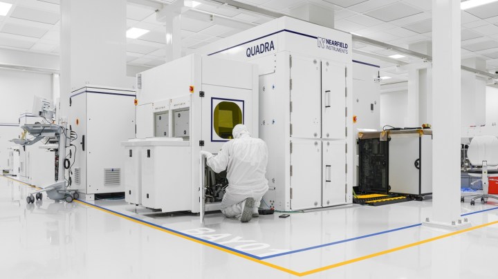
The company’s QUADRA platform uses an extremely small AFM probe tip to scan inside nanoscale structures. But as trenches become narrower, the probe itself must also become thinner to enter the structure. Extremely narrow probes, however, can bend under atomic interactions along the sidewall, distorting measurements and limiting accuracy.
“When the tip is very narrow, even if you manage to go inside the trench, it does not give you the true structure,” Sadeghian said. Nearfield’s approach adds torsion-sensitive sensing designed to directly measure those sidewall interactions rather than treating them as measurement noise.
The goal is not simply a better profile measurement, but a more complete representation of buried structures during inline manufacturing. “Instead of giving just one profile, we give a full image,” Sadeghian said, comparing the difference to seeing a single cross-section of a wall versus viewing an entire city in three dimensions.
The company says the technology can inspect structures with openings as small as roughly 15 nm and aspect ratios exceeding 100 nm in depth while remaining compatible with inline semiconductor manufacturing flows.
Metrology becomes a scaling bottleneck
Sadeghian believes improved sidewall control could eventually influence not only manufacturing yield, but also energy efficiency in large-scale AI infrastructure. “If I control the sidewall better, I need less voltage to power that chip,” he said. “Imagine scaling this up with AI data centers and millions of these chips.”
Inline non-destructive inspection could also reduce the number of wafers sacrificed for destructive analysis and lower the amount of supporting failure-analysis infrastructure required inside fabs.
As semiconductor manufacturing becomes more complex, metrology itself is becoming a larger and more strategically important part of the production flow. “The number of metrology and inspection steps in a flow is increasing,” Leray said. “And proportionally, the metrology and inspection are increasing more.”
Neither imec nor Nearfield believes a single inspection technology will solve every future process-control challenge. Instead, the industry increasingly appears to be moving toward combinations of optical, e-beam, X-ray, AFM, and data-analysis systems working together to create more complete visibility inside advanced semiconductor structures.
For Leray, the semiconductor industry’s largest unresolved challenge is the ability to fully see what manufacturers are building inside increasingly opaque 3D devices. And that challenge, he added, is only becoming harder. “Because it’s deep. It’s opaque. And what we need to detect is small.”