Necessity is the Mother of Invention: Huawei Replaces Moore’s Law With Her’s Law
We now know what China’s been working on to counter U.S. sanctions on EUV technology.
At IEEE ISCAS 2026 in Shanghai yesterday (May 26), Huawei president He Tingbo presented China’s answer to U.S. chip manufacturing sanctions, named after her: Her’s Law (Huawei has been writing “Her’s Law” rather than “He’s Law” to encourage the proper pronunciation).
Per He’s presentation, Her’s Law offers a replacement for Moore’s Law. Moore’s Law relies on geometric scaling that is off-limits to Chinese chipmakers and foundries because they are denied access to EUV technology due to U.S. sanctions.
Knowing that necessity is the mother of invention, as the saying goes, critics of U.S. sanctions feared that restricting access to EUV in 2020 would force China to innovate in other directions. We now know what China’s response to those sanctions looks like—as widely expected, Huawei and SMIC have accelerated other parts of the roadmap to try to compensate for a lack of access to geometry shrinkage.
The upshot is that Huawei wants to reach the equivalent of the rest of the industry’s 14Å node performance by 2031, something Intel expects to achieve by 2027 and TSMC by 2028, placing Huawei about three years behind.
From He Tingbo’s ISCAS keynote slides. Huawei’s roadmap shows the company achieving density and clock frequency parity with Western 14Å nodes by 2031. The reason for the big jump in performance between 2030 and 2031 is unclear. (Source: Huawei)
3D stacking
How will Huawei achieve its aggressive targets? The crux of it is the company’s accelerated 3D stacking roadmap.
The slide below from AMD’s Hot Chips 33 presentation (in 2021) has been widely shared on social media to illustrate the industry-wide roadmap for this technology. Silicon Valley chipmakers are still edging toward the first stage.Huawei wants to leapfrog several stages ahead by 2031.
A slide illustrating 3D stacking stages from the perspective of AMD (Source: AMD/Hot Chips 33)
Huawei calls its new 3D stacking technology LogicFolding. The aim is to speed things up by reducing the physical length of the wires (reducing parasitic RC) between components in the critical timing path. This is achieved by stacking dies vertically, back-to-back, and bonding between connections to components on each die.
However, this requires an extremely aggressive hybrid bonding pitch. He said in her keynote that the magic number is a pitch of 2 µm and that the bonding pitch on Kirin 2026 (Huawei’s forthcoming update to its flagship mobile SoC) has reached this level or below. Reducing the pitch to this level is crucial to enabling hybrid bonds to become part of the critical timing path.
Shorter paths depend on aggressively reduced hybrid bonding pitch. (Source: Huawei)
He said in her keynote that geometry scaling per Moore’s Law had taken three years to lift transistor density from 126 to 155 MTr/mm². In 2026, He said LogicFolding will take it all the way to 238 MTr/mm², in a single step. This framing is perhaps a little disingenuous; Huawei’s transistor density is really per cubic millimeter, not per square millimeter, since the dies are stacked vertically. The transistors are not any denser on the individual dies. Ultimately, though, “density” is just semantics—He said that SoC P-core power efficiency jumped 41% and maximum clock frequency rose by 12.7% for a LogicFolding design compared to a 2D version of Kirin 2026.
Accelerated development
To be clear, advanced 3D stacking techniques such as LogicFolding are on the roadmap for the entire industry, but Huawei has accelerated their development to bring them forward in time. Chipmakers outside China haven’t needed to—at least not yet—since they are still able to rely on process node shrinkage via EUV lithography. For comparison, current state-of-the-art commercial projects such as AMD’s V-cache and Intel’s Foveros are in the region of 8-10 µm hybrid bond pitch.
Advanced 3D stacking has been in development across the industry for decades, and development roadmaps are well understood, but commercializing requires investment to manufacture in volume, repeatably, and reliably, at the right cost point, and to develop tools. He’s keynote suggested some of these areas are more advanced than others (“we warmly welcome partners and experts in [methodologies and tools] to join us for future improvements,” she said), but it seems certain that Huawei is far ahead of its competitors in this area at present.
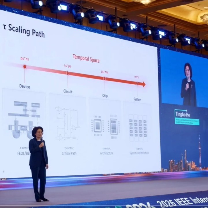
He suggested a reframing of industry progress as part of Her’s Law, which she called τ scaling. Put simply, τ scaling restates the problem such that progress isn’t tied to transistor density (even though Huawei claims advantages in density); rather, any form of progress in terms of speeding up compute, or memory access, or system performance, can be considered an advancement, no matter how it is achieved. This fits with higher-level industry trends toward accelerated computing, domain-specific architectures, and a whole host of system-level scale-up and scale-out technologies in the age of AI.
He Tingbo presents τ scaling at ISCAS 2026. (Source: Huawei)
While the underlying hybrid bonding technology Huawei has developed is impressive, other parts of the industry are prioritizing a different path and will develop their own versions of 3D stacking in parallel with geometric scaling. Huawei’s announcement, therefore, should not be viewed as China ‘catching up.’ Silicon Valley’s lead has been shortened, but that may prove to be temporary. Rather, it seems clear this announcement is intended to focus China’s semiconductor ecosystem around a single technological trajectory, with the hope of accelerating it, EUV or no EUV.
Read also:
Huawei’s answer to Moore’s Law without EUV promises 14A performance by 2031.
RELATED TOPICS:3D SILICON STACKING, CHINA, FOUNDRY, HUAWEI, HYBRID BONDING, SEMICONDUCTORS
COMPANIES:HUAWEI
_Sally Ward-Foxton covers AI for EETimes.com and EETimes Europe magazine. Sally has spent the last 18 years writing about the electronics industry from London. She has written for Electronic Design, ECN, Electronic Specifier: Design, Components in Electronics, and many more news publications. She holds a Masters' degree in Electrical and Electronic Engineering from the University of Cambridge._Follow Sally on LinkedIn
2 comments
Santhoff2026-05-28 15:05:52
How are they planning to deal with heat dissipation and with contacts at 2um? A pitch of 2um along with the anticipated thermal issues appears to present some significant issues.
Santhoff2026-05-28 15:05:53
How are they planning to deal with heat dissipation and with contacts at 2um? A pitch of 2um along with the anticipated thermal issues appears to present some significant issues.