業界ニュース
半導体・電子部品業界の最新ニュースをお届けします
LPDDR6 Roadmap Leads to the Data Center
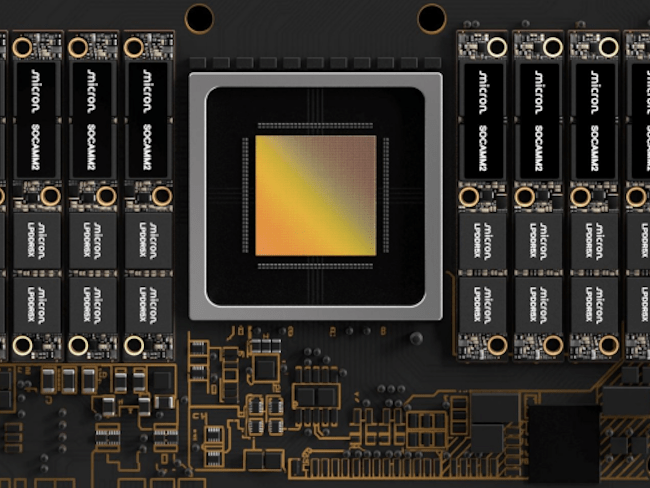
The upcoming update to JEDEC’s LPDDR6 will squeeze in several features that address the memory’s increasing popularity in AI data centers. For years, LPDDR was associated with smartphones, tablets, and ultra-thin laptops, but now a great deal of supply is being eaten up by memory-hungry AI data centers as they look to reduce power consumption Since releasing the “foundational” JESD209 6 in July 2025, JEDEC’s JC 42.6 Subcommittee has been focused on extending the LPDDR6 standard beyond mobile platforms to support selected data center and accelerated computing workloads that need power-efficient, high-capacity memory. Increasing performance while reducing power consumption is fundamental to any JEDEC memory standard, Hung Vuong, chair of the JC-42.6 Subcommittee for Low Power Memories, said in a briefing with EE Times. Data center customers are especially interested in LPDDR. “This revision of LPDDR6 will focus a lot of features on their needs,” Vuong said. One key feature will be a narrower x6 per-die interface, which enables higher capacities, said Osamu Nagashima, the subcommittee’s vice-chair. As far as bandwidth goes, it’s not so much of a big jump—perhaps 10 to 20% improvement from the previous iteration. “They can double the densities,” he said. LPDDR6 SOCAMM, such as those offered by Micron Technology, are well-suited for AI systems due to their small footprint while offering 2.5× the bandwidth of conventional modules and consuming about one-third less energy. (Source: Micron) Moving to a non-binary interface width and an additional x6 sub-channel mode allows more die per package and higher memory capacities per component and per channel. Nagashima said the goal is to reach 512GB density, which is beyond the current LPDDR5/5X maximum, to address the ever-growing memory capacity requirements of AI training and inference workloads. The upcoming update will also include an LPDDR6 SOCAMM2 module standard, designed to advance the compact, serviceable module form factor and offer a clear upgrade path from today’s LPDDR5X SOCAMM2 modules. SOCAMM is well-suited to address AI systems’ energy and space constraints by offering 2.5× the bandwidth of conventional modules, while consuming about one-third less energy. Earlier this year, Micron Technology released its 256GB SOCAMM2, a data center–class modular LPDDR5X memory module for AI infrastructure. JEDEC is also nearing completion of a standard for LPDDR6 processing-in-memory (LPDDR6 PIM) technology, which complements the broader LPDDR6 roadmap. Vuong said the LPDDR6‑PIM embeds compute logic directly inside the memory chip, letting the memory perform calculations instead of just storing data. “The idea is to offload some processing into the memory.” Nagashima said this reduces data movement between CPU/GPU and RAM, which is the main bottleneck for AI workloads. while reducing power use. Vuong said LPDDR has been transitioning to become a data center memory over the last five years—it’s gone from being primarily a mobile, solder-on solution for smartphones to moving into client computing as companies such as Dell, Lenovo, and HP saw the value of LPDDR5 technology. He said LPDDR6, as well as SOCAMM, has caught the attention of data center customers as power consumption becomes an increasingly important metric. “AI and data centers are really driving—or straining—the ecosystem right now.” Vuong said there’s been significant pressure from those users to update the LPDDR6 standard, but also a lot of cooperation to advance it. “Most of the features are defined already,” he said. “We’re just crossing the Ts, dotting the Is, and making sure we didn’t miss anything.”

Taiwan Minister Emphasizes Collaboration and Future Focus on Photonics, WBG, and Quantum
In an exclusive video interview, NSTC Minister Wu shares Taiwan’s four-pillar shift from chipmaker to AI enabler. As AI reshapes the technology landscape, Taiwan remains at the center of the global semiconductor ecosystem. In this exclusive video interview with EE Times, Minister of the National Science and Technology Council (NSTC) Cheng-Wen Wu outlines the nation’s strategy for sustaining leadership amid rising geopolitical pressures, resource constraints, and accelerating demand for advanced computing technologies. Watch the full interview here: Alternatively, you can listen to the audio below, where Wu also talks about mitigating scarcity and geopolitical pressures, plus the success of its science park ecosystem in encouraging Taiwan’s startups: Audio 3 The discussion explores Taiwan’s vision beyond semiconductor manufacturing, highlighting four strategic pillars: continued investment in advanced manufacturing and R&D, deeper international collaboration, expansion into next-generation applications such as robotics, autonomous systems, and space technologies, and a commitment to sustainable industrial growth through energy efficiency and net-zero initiatives. A major focus of the conversation is silicon photonics, which Taiwan sees as a foundational technology for enabling future AI infrastructure. The interview examines how Taiwan’s manufacturing expertise, combined with partnerships across the U.S., Europe, Japan, and other global technology hubs, could help overcome scalability challenges and accelerate the development of all-photonic networks. The discussion also addresses emerging opportunities in quantum computing, advanced packaging, power electronics, and compound semiconductors, while providing insight into how Taiwan is balancing economic growth with environmental stewardship and resource management. Ultimately, Wu’s message is that while Taiwan has focused on manufacturing, it is comprehensively focused on transitioning from a pure hardware manufacturer to a global enabler of multi-domain innovations. Backing this up, Wu talked about the policy framework that underpins this, built around four central pillars designed to sustain and build upon Taiwan’s current economic momentum: Maintaining advanced manufacturing dominance:continuing aggressive public and private R&D investment to stay at the cutting edge of semiconductor and AI server manufacturing. Strengthening international collaboration:accepting that Taiwan cannot maintain its edge in isolation. The goal is to collaborate deeply on scientific research, tools, materials, and chemicals with global, democratic, and free-market countries. Socio-economic application and expansion:spreading the wealth of Taiwan’s manufacturing power to benefit other critical, emerging fields, including AI robotics, space industries, autonomous vehicles, drones, and traditional service sectors like agriculture, education, and transport. Net-zero and sustainability commitments: engineering cleaner manufacturing processes, preserving the ecology of science parks (even aiming to bring back endangered species), and investing heavily in power electronics to slash global tech energy consumption.

Photonics: A Foundational Scaling Layer for AI-Era Computing
Photonics is becoming a foundational scaling layer for AI-era computing. Once discussed mainly in telecommunications and long-haul networking, optical technology is now appearing across the semiconductor ecosystem: inside data centers, at the edge of packages, between chips, across racks, and as part of computing itself. The reason is simple. The hardest problems in computing are no longer confined to the transistor. They are system-level problems: How to move more data over longer distances with lower latency, less power, and stronger security. That shift is changing how the industry thinks about Moore’s Law. For decades, progress was measured by what could be packed onto a single chip. AI is stretching that definition. The new unit of performance is often not a processor, but a cluster. Large language models and generative AI systems routinely exceed the resources of a single server, requiring groups of accelerators to behave like one computer. In that environment, scaling is limited as much by communication and memory access as by raw compute. Optical interconnect is emerging because AI computing has changed. Training, inference, retrieval, reasoning, and agentic applications place different stresses on memory, networking, and accelerators. As clusters grow, GPUs and AI accelerators must exchange parameters, activations, key-value caches, and intermediate results fast enough to keep utilization high. Every idle accelerator represents expensive silicon and power doing nothing. Copper remains useful over short interconnect lengths, but as bandwidth rises and distance grows, electrical signaling becomes harder to scale without penalties in loss, power, density, or complexity. Memory is becoming the critical battleground. AI systems are often described as compute-hungry, but modern inference is increasingly memory-hungry. Long-context models and reasoning workloads generate and reuse large key-value caches. Agentic AI intensifies this pressure by requiring systems to preserve context across repeated reasoning steps, coordinate multiple tools and workflows, and support many concurrent users or autonomous agents. When memory is constrained, systems may shorten context, move data through slower tiers, reduce concurrency, or accept lower output quality. The business impact is direct: fewer high-value tokens per watt, per dollar, and per unit of installed infrastructure. This is why memory cannot remain strictly local. High-bandwidth memory attached to an accelerator is valuable, but finite and expensive. As workloads scale, systems need access to larger shared memory pools without forcing every byte through a slow storage-like path. Protocols such as Compute Express Link (CXL) enable low-latency, coherent access to pooled and disaggregated memory. Paired with optical networking, this model can extend memory across boards, servers, and racks while preserving the semantics needed by CPUs, GPUs, AI accelerators, and FPGAs. Optics can turn memory from a stranded local resource into a composable system resource. The same logic applies to compute scaling. AI workloads rely on shared memory footprints and fast communication across a distributed system, not just compute inside one box. A rack of accelerators is useful only if they can be programmed and fed as a coordinated machine. Optical links and optical switching excel at providing the bandwidth, latency, reach, and topology flexibility needed to connect devices at multiple levels: chip-to-chip, package-to-package, rack-to-rack, and cluster-to-cluster. Over time, this points toward data centers whose topology can be shaped around workloads rather than fixed by copper traces and static cabling. Optical computing adds another layer. Not every workload is suitable for optics, but many high-value operations in AI and scientific computing are dominated by linear algebra and parallel data movement. Photonic processors can perform certain matrix and vector operations with very low latency and attractive energy characteristics. The most successful designs are likely to be workload-first rather than physics-first: pairing optical processing with electronics, software stacks, compilers, and application frameworks so the right parts of the workload run in the right medium. Photonics also has underappreciated advantages outside speed and power. Optical media are immune to electromagnetic interference because signals are carried by light rather than electrical current. They also do not radiate electromagnetic signals in the same way metal interconnects do. That matters in electrically noisy environments, defense applications, medical infrastructure, and anywhere signal leakage or interference creates risk. While no technology is automatically secure, optical links reduce certain electromagnetic side channels and can make passive interception more difficult than with conductive media. The next phase of photonics will be defined by breadth. Pluggable optics, co-packaged optics, optical I/O chiplets, optical circuit switches, CXL-enabled memory fabrics, and optical accelerators all address different parts of the same system-level problem. AI has exposed the limits of moving data with electrons alone, but the implications extend far beyond AI. As data grows faster than conventional infrastructure can comfortably move it, photonics will continue expanding its role as a foundational scaling layer for AI-era computing, especially as data centers, advanced memory systems, and next-generation workloads place unprecedented demands on bandwidth, latency, power, reach, and security.

Physical AI Pushes Chipmakers Up the Value Chain
AMSTERDAM, The Netherlands — At TSMC’s European Symposium, senior executives from some of TSMC’s lead customers talked about how AI is changing the shape of their products and businesses. STMicroelectronics (ST) CEO Jean-Marc Chéry said that the European MCU giant is transforming itself to take advantage of the opportunity AI presents. “ST [will] adapt ourselves, transform ourselves in order to take advantage of this AI journey, and convergence in ST’s two key markets,” he said. ST’s two key markets up to now are automotive and industrial, with selective participation in consumer electronics and communications infrastructure. ST needs to move from a component supplier to an application enabler for customers, which will require solid know-how in system-level engineering, Chéry said. “The problem is, to develop a solid know-how in systems if you have infinite systems is basically impossible,” he said. “The good news is, we are seeing some convergence between the different industries. One good example of this convergence is physical AI.” This new category of “physical AI” is a convergence of sectors previously called mobility and industrial autonomy, Chéry said. Architectures for EVs, industrial robots, and humanoid robots have a reasonable amount of crossover; all use central computing with zonal control with a sensor, driver, switcher, and controller. “The challenge is to understand where you can optimize new components offered or the platform you develop in order to reuse and develop your knowledge on systems, for each of these systems or subsystems,” he said. This knowledge has completely changed the organization of ST, Chéry said. The company has moved from a traditional automotive power/analog/MCU vendor to segment marketing by vertical, with a strong systems-engineering perspective. Rather than discussing individual performance, the aim is to tell customers which products are required to achieve a specific level of robot hand strength or sensitivity. ST also works with its partners to digitally tweak components for specific physical AI use cases, such as robotics. “This is a totally different approach,” he said. “This approach is possible because we see convergence everywhere, because we can reuse this system approach on humanoid, industrial robots, and electric cars.” The company has been working over the last two years to switch from a component provider to one that can take advantage of “this fantastic journey of AI,” Chéry said. “It’s very exciting, I have to say—it’s a major transformation,” he said. “What will happen in the next five years is clearly a competitive landscape displacement because doing all these activities using agentic AI, transforming the company itself, is certainly the most passionate period I have ever faced in my 42-year career in Silicon Valley.” A slide from Jean-Marc Chéry’s presentation. The new physical AI category involves the convergence of mobility, industrial automation, and humanoid robotics sectors, he said. (Source: STMicroelectronics) Infrastructure requirements The industry is actually underestimating the need for AI infrastructure, said Jeetu Patel, president and chief product officer at Cisco. “We are witnessing a profound change in society with what’s happening with AI, and it’s proliferating everywhere in all of our lives,” he said. “Despite all the hype, what we’re starting to see is that we’ve underestimated the infrastructure requirements for AI, and there’s just not enough power, compute, network bandwidth capacity in the world to satiate the needs of AI.” The shift to agentic AI will put intense pressure on infrastructure, given AI agents’ patterns of usage are very different from humans using AI chatbots, Patel said. “Chatbots had a very spiky pattern of usage from a network band’s perspective,” he said. “Asking a question, getting an answer, was very much at human speed… agents have a much more persistent, sustained pattern of usage for infrastructure demands—they’re far hungrier for infrastructure than chatbots.” Agents also work 24/7 at machine scale and speed and are showing an order-of-magnitude higher infrastructure consumption than chatbots, Patel said, and the figure is 450% higher than infrastructure consumption when a human performs the same tasks. “No matter how much infrastructure you feel that will be needed in the world, you are underestimating the capacity that’s going to be needed,” he said. The result is we are entering a networking super-cycle, Patel said. Rapidly accelerating infrastructure build-out has already started, but networking at every sale will require whole new classes of technology. This includes 3D stacking, co-packaged optics, advanced power supply techniques, and thermal dissipation technologies, Patel added. Infrastructure demand patterns from AI agents and physical AI are totally different from chatbots (Source: Cisco) Lifecycle management “AI is moving full speed into our lives in all ways,” said Nordic Semiconductor CEO Vegard Wollan. “Edge compute, far edge processing, AI inference, NPUs—they are changing the game at the edge, where new hardware and software requirements are developing extremely fast. At Nordic, we believe that this transformation is going to be present on every battery-operated, battery-powered device very soon.” Like ST, Nordic is also making the leap from a chip company to system supplier, Wollan said. “Last summer, we made a strategic shift from being a chip company to a complete wireless solutions technology partner for our customer base. That means focusing on the pillars of world-class hardware, embedded software, and life cycle services. We added life cycle management to our portfolio, to the fleets of millions of connected products that are out there.” While there were multiple reasons to add lifecycle management to its portfolio, the key reason was to support physical AI applications as they permeate all embedded devices, Wollan said. Nordic is also embracing AI for its new development tools, where the company has added AI agents and AI-assisted development to all phases of the product lifecycle, from prototyping to deployment. “You have the best and most knowledgeable support engineer behind you, always,” Wollan said. “It answers, supports you immediately, writes a lot of your code with no delay. This is, of course, about our customers bringing end products to the market a lot faster.” This speedup is actually happening, Wollan added, despite relatively complex development cycles that are subject to wireless connectivity regulations, certifications, and qualifications. “We can bring [the development cycle] down from 20 months to 15 months to 10 months to 5 months,” he said. Nordic Semiconductor has added AI agents that can help designers at every stage of the development cycle. (Source: Nordic Semiconductor)
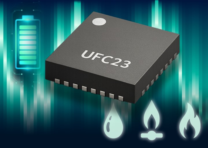
ScioSense Launches UFC23 Ultrasonic Flow Converter for High-Precision, Ultra-Low-Power Smart Metering
Dutch sensor manufacturer ScioSense has launched its fourth-generation ultrasonic flow converter (UFC), called UFC23, for water, heat, and gas metering applications. The company said the new sensor combines high measurement precision, improved offset stability, and ultra-low power consumption for battery-powered smart metering systems. The company’s latest product is designed as pure front-end architecture without an on-chip CPU, allowing OEMs to perform flow calculations on their preferred host microcontrollers from companies such as STMicroelectronics, NXP, and Renesas. The company said this approach gives meter manufacturers greater flexibility in system design while improving analog front-end performance. EE Times interviewed Norbert Breyer, director of marketing and product management at ScioSense, who said: “We want to relieve customers from developing the analog front end for an ultrasonic meter. With our separate approach, where the front end manages the flow measurement and the customer has full flexibility on the microcontroller side, users can move to the latest generations of microcontrollers whenever they want. We are also cooperating with the suppliers to develop sample code for their microcontroller platforms.” Breyer explained that earlier products such as the GP30 and AS6031 included small proprietary CPUs capable of handling flow calculations internally. These products also offered firmware-integrated versions for customers with limited software expertise. However, newer smart meter designs increasingly require higher processing capability and bidirectional flow measurement, pushing customers toward performing flow calculations using external microcontrollers. “Customers told us that they liked the GP30 and AS6031 because of their strong performance, but they wanted similar performance without the CPU,” Breyer said. “That is why we introduced UFC23.” The UFC23 integrates ultrasonic transducer drive functions, signal capture, and high-precision time-of-flight extraction. It also includes a programmable gain amplifier with increased gain and bandwidth, a programmable ultrasonic burst generator operating up to 4.40MHz, and batch measurement capability that allows the sensor to collect up to 12 measurement bundles before waking the host controller. The UFC23 operates with a standby current of typically 0.8 microamps and an operating current as low as 6.60 microamps at an 8Hz sample rate. The converter supports both 3.3 V single-ended drive for water applications and full-bridge drive for gas applications. The ScioSense UFC23 time-to-digital converter IC, designed for ultra-low-power flow measurement in utility meters and industrial applications. (Source: ScioSense) ScioSense is focusing heavily on low-power operation because smart meters operate using batteries that are expected to last between 10 and 20 years. Breyer said the company’s solutions typically operate at current consumption levels between 5 and 8 microamps. At 88Hz operation, current consumption is around 6.50 microamps and can be reduced to approximately 4 microamps using adaptive sampling algorithms. “The target lifetime for these products is 20 years,” Breyer said. “With a AAA cell, if the microcontroller is power-efficient, operation for 20 years should be achievable.” Breyer explained that the company’s UFC front-end chips connect directly to ultrasonic spool pieces and transducers. Data can then be read through serial peripheral interface (SPI) using the customer’s central microcontroller. Ultrasonic meters replace mechanical turbine meters Breyer pointed out the trend of ultrasonic meters replacing traditional mechanical turbine meters because they provide higher sensitivity, longer lifetime, and lower maintenance requirements. “Dirt and contaminants in water can eventually stop the turbine from rotating, resulting in measurement errors and shorter operating life. With ultrasonic technology, customers want to replace this mechanical sensor with a static sensor. There are no moving parts. Dirt in the water cannot cause the mechanical turbine to get stuck because nothing rotates,” he explained. Breyer said ultrasonic meters can detect flows as low as 0.50 liters per hour, compared to approximately 5 liters per hour for mechanical turbine meters. This allows utilities to identify dripping taps, leaking pipelines, and faulty toilet valves much earlier. He added that mechanical turbine meters can show errors of around 30% after six years because aging affects turbine movement. “Utilities therefore benefit financially from replacing mechanical meters with ultrasonic meters because they can conserve water and bill more accurately,” Breyer said. The UFC23 supports applications including smart water meters, heat meters, gas meters, water heaters, pump control systems, smart faucets, and leak detection systems. ScioSense said samples and evaluation kits are already available through distribution partners. Challenges in ultrasonic metering According to Breyer, one of the biggest technical challenges in ultrasonic metering is measuring time-of-flight differences with picosecond-level precision. In ultrasonic meters, two transducers send ultrasonic waves in opposite directions through the fluid. The system calculates flow by measuring changes in travel time. For small meters, the time of flight is typically around 30 microseconds, while larger meters may operate between 70 and 100 microseconds. “The latest market trend is toward a 1:1000 measurement ratio, which requires precision around 10 picoseconds,” Breyer said. He added that ScioSense front ends currently achieve approximately 35 picoseconds in single-shot measurements, while averaging further improves performance. The offset stability is ±7 picoseconds using 128-sample averaging, with drift below 10 picoseconds across a temperature range from 0°C to 50°C in a typical DN15 water meter configuration. “We are focusing on maintaining measurement stability across temperature variations because temperature stability directly affects metering accuracy,” Breyer said. Business operations Water metering currently accounts for around 70% of ScioSense’s flow business, while heat contributes around 20% and gas approximately 10%. He expects the ratio to move closer to 2:1:1 between water, heat, and gas in the medium term. “While the heat meter market remains relatively stable, gas metering demand in Europe has slowed because of reduced dependence on gas-based heating following the war in the region. However, China continues showing strong interest in gas metering,” he said. Breyer said Europe currently represents the strongest ultrasonic metering market, with an estimated 50% of the sector already transitioning toward ultrasonic technology. He added that China has rapidly increased ultrasonic meter adoption during the past five years, while India is now showing strong interest. “America is also a strong market, and many leading manufacturers are shifting toward ultrasonic technology. We have many Indian customers beginning development of ultrasonic water meters,” Breyer said. ScioSense operates as a fabless semiconductor vendor. The company uses a German foundry with production carried out in Asia. “We cooperate with globally active companies that can easily handle high production volumes, so manufacturing capacity is not a limitation,” he said. The company works directly with OEMs globally rather than electronics manufacturing services providers. The sensor manufacturer provides evaluation boards, demonstrator software, and sample code for Arduino and STMicroelectronics microcontrollers through GitHub. Breyer said the company works with distributors including DigiKey, Mouser, Avnet India, Future Electronics, and WT Microelectronics. Customers can purchase individual quantities or evaluation kits through these partners. “For higher quantities, we typically sell in reels containing 1,000 pieces,” he said. Technical support is generally provided directly by ScioSense because distributors may not possess the same level of system expertise. ScioSense is researching water quality sensing technologies as a possible future expansion beyond conventional flow metering. Breyer said the industry is still determining how water quality should be defined and measured. “It could involve parameters such as pH, chlorine, carbon dioxide, or other factors. At the moment it is still at the research stage,” he said.
TSMC Defends Transistor Scaling Amid Huawei’s ‘Her’s Law’ Proposal
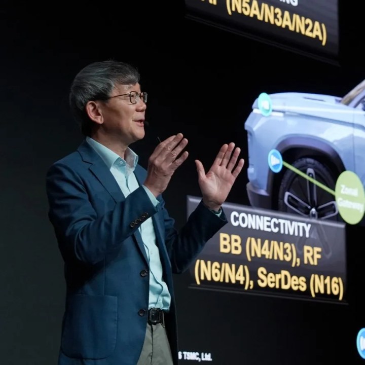
AMSTERDAM, The Netherlands — At TSMC’s European Symposium, Kevin Zhang, senior VP and deputy co-chief operating officer at market-leading foundry TSMC, responded to questions from reporters about Huawei’s proposal to stop measuring industry progress on transistor density. Huawei proposed Her’s Law, analogous to Moore’s Law, based on Tao scaling, a method of measuring industry progress in terms of overall speedup rather than purely on transistor density. Huawei does not have access to EUV machines necessary to shrink transistor geometries beyond 7-nm process nodes. Asked about Huawei’s Tao scaling theory, Zhang said that while he had not looked into it in detail, Tao scaling appears to be a matter of 3D integration, which can bring different functions closer together to reduce delays between chips. “I think that the concept [of 3D integration] has been around in this industry for long enough,” he said. “This is something, obviously, we’re going to continue work with our customers to drive forward. That’s how I look at it.” Fundamentally, the transistor is still critical, Zhang said. “Remember, all the computation is done at the transistor level, so don’t forget how important the transistor is,” he added. “If you look at the overall R&D effort, transistor development continues to consume the most R&D effort to drive the next generations of technology. Transistor technology takes tremendous effort.” Kevin Zhang presents at TSMC’s European Symposium in Amsterdam (Source: TSMC) Transistor technology scaling on its own can give you 30% better energy efficiency when moving from N2 to A14. “That’s the number, it’s absolutely significant,” Zhang said. To illustrate, Zhang pointed towards a growing movement in the data center world to deliver 800 V directly to racks, which means replacing entire power delivery systems. This is a considerable task which improves energy efficiency by only low-single-digit percentage points, Zhang said. By comparison, shrinking transistor geometries between N2 and A14 process nodes would reduce power by 30%. Transistor geometry shrinking as practiced by TSMC is the industry’s key vector for increasing transistor density today. TSMC has access to EUV technology and its roadmap is based on shrinking the geometry of its transistors. In the ISCAS keynote, Huawei claimed their 3D stacking method increases density per square millimeter despite not adding more transistors to any individual die. Zhang was generous when asked about the Chinese hyperscaler’s new definition of “density.” “Density, in my view, is no longer measured in two dimensions,” he said. “It’s measured by space. The vertical dimension also comes in when you talk about overall space.” Die stacking is certainly an innovative way to increase computation density, Zhang said. “Stacking gives you another dimension to continue to increase the computation per cubic centimeter,” he said. “When you build a data center, you really think about the three-dimensional space, that’s how important it is.” TSMC is looking at technologies like CFETs (complementary field-effect transistors) for future transistors. Zhang said CFETs are attractive precisely because they are stacked in three dimensions. CFETs comprise a p-type FET stacked on top of an n-type FET, within the same die, effectively building two transistors in the space previously occupied by one. TSMC’s European venture, ESMC in Dresden, is on track, Zhang said. The foundry leader broke ground almost two years ago for the fabs, which will focus on automotive and industrial products. Tools should be installed in the new fabs by 2027, but the overall ramp schedule will be based on market conditions and customer needs, the company said.

High-Voltage GaN Bi-Directional Switches: Strong Performance, Simpler to Use
The demand for more efficient power solutions continues to put pressure on designers to optimize system design without compromising performance. Read how you can simplify high-voltage power conversion and reduce system cost, size and complexity for a range of demanding applications with GaN BDS. High-voltage GaN bi-directional switches enable implementation of single-stage power converters with true bi-directional voltage blocking and current conduction in a single device. To view this content, please fill out the form below. "" indicates required fields Facebook This field is for validation purposes and should be left unchanged. Name First Last Business email Job Title Company Job Function Industry State / Country State / Province / Region Country By clicking on View Now! - [x] By clicking on Download Now, I agree that my information may be shared with Renesas, who may email me about industry updates,products or services. CAPTCHA By submitting this form you agree to AspenCore's Privacy Policy and Terms of Use 0 comments

Early Memory Contention Checks Reduce IC Design Risks
Invisible risks lurking in memory design can quickly derail even the best planned silicon projects. As system-on-chips (SoCs), AI accelerators, and high-performance graphics devices grow in complexity, memory bottlenecks and reliability hazards like contention aren’t just theoretical—they’re a leading source of costly delays and hardware failures across the electronics industry. Early detection emerges as an industry imperative Memory sits at the heart of every modern electronic system, whether in safety-critical automotive applications, hyperscale data centers, or the resource-constrained edge. The relentless demand for greater capacity, higher throughput, and improved reliability pushes designers to work under compressed schedules, even as system complexity ramps upward. Custom DRAM, high-speed SRAM, nonvolatile flash, and embedded memory blocks all present special challenges, each requiring careful integration across advanced architectures, tight power budgets, and sophisticated peripheral logic. The diversity of architectures intensifies this complexity. Each memory type—whether high-bandwidth memory (HBM) for graphics, SRAM for rapid access, or VRAM for specialized caching—introduces its own set of integration risks. Among the most insidious, memory contention occurs when multiple domains or drivers vie for control of a single node—a hazard that can look different depending on the architecture involved. For example, contention may stem from insufficient isolation between banks in HBM, or conflicting enable signals in SRAM blocks(Figure1). Despite their differences, these forms of contention often escape detection until late in development, when their impact can be far-reaching and costly to fix. Figure 1: Complex signal sharing in advanced memory architectures increases the likelihood of contention. Red arrows demonstrated where conflicting control could arise. Schematic-level checking: A shift-left solution for memory reliability To address these bottlenecks proactively, leading engineering teams are embracing schematic-level, pre-layout memory contention checking—a shift-left methodology that brings reliability analysis into the design flow’s earliest stages.Using schematic-level checking tools,designers can fix issues when edits are easy, root causes are clear, and design intent is still malleable(Figure 2). Figure 2: Left side: A traditional flow.Contention checking happens after layout. Right side: Shift-left flow shows schematic-level contention check catching issues early, before layout begins. Early schematic-stage analysis brings significant advantages, both technical and economic. By catching contention before layout, designers can ward off physical damage from opposing outputs, preserve logic reliability, and ensure signals remain deterministic—avoiding“X” states that can ripple unpredictably through the rest of the system. Tackling these risks early on reduces the need for late-stage redesigns and hardware re-spins, offering substantial cost savings.Schematic-level analysis also extends simulation coverage,flagging edge cases that dynamic test benches might not exercise.Perhaps most crucial, designers gain visibility into potential high-current states and heat sources that emerge unexpectedly, giving them more freedom to optimize for power integrity before the physical design is set. Teams benefit not only from error prevention, but also from improved collaboration between analog and digital domains. Memory contention issues often involve intricate interactions between these domains, especially at interfaces and across multiple clock and power regimes.By surfacing these problems early, schematic-level checking enables more productive collaboration between engineering teams and allows potential integration problems to be resolved before they harden into costly, late-stage showstoppers. Tackling advanced integration and evolving risks The complexity of today’s memory landscapes is unprecedented, encompassing a mix of cell technologies, clock domains, and power rails. Integration challenges intensify as peripheral circuits—such as address decoders, power gating modules, and arbitration logic—become more sophisticated. Design missteps at the schematic level—whether due to aggressive timing closure, novel clock architectures, or misconfigured interfaces—can swiftly propagate into widespread contention. An automated schematic verification tool,such as Siemens Insight Analyzer,identifies conflicts resulting from simultaneous activation of multiple memory banks, overlapping power domains, or rare leakage paths from incorrect tristate logic(Figure 3).The tool’s state-aware analysis exposes cases that traditional simulation fails to find,such as asynchronous clock domain glitches placing conflicting logic levels onto shared nets. Using block-level “black boxing,” teams can focus on newly introduced logic and integration pathways, efficiently targeting areas most likely to conceal schematic contentions. Figure 3: Schematic-level detection of logic contention in memory periphery circuits. The Insight Analyzer tool identifies multiple drivers, sourced from distinct asynchronous clock domains that simultaneously place conflicting logic levels onto the shared CLKO net. Even memory arrays previously verified in other products may create unexpected issues when ported to new contexts. As functional safety and silicon success on the first try become industry imperatives, schematic analysis has become an essential layer of defense. Modern SoCs and accelerators frequently incorporate several heterogeneous memory banks, each with dedicated controllers and power domains—exponentially increasing the chances for subtle, undetected interaction. Delivering cost, schedule, and reliability gainsA Moving design intent checks earlier unlocks new potential for architectural optimization. Design engineers can freely experiment, reshape block hierarchies, and refine control topologies, informed by actionable feedback rather than costly surprises. With schematic-level checking, teams gain confidence in bounding delays, achieving safety compliance, and managing functional resources. The net result is more reliable, efficient, and competitive memory systems that meet demanding market timelines. The bottom line is that early, automated schematic-level contention analysis is transforming memory design from a game of chance into a discipline rooted in engineering certainty. By leveraging shift-left practices, teams detect and resolve bottlenecks early, improve predictability, and avoid disruptive late-stage changes. As complexity and competitive pressure both rise, equipping design flows with advanced, pre-layout checking capabilities has become essential to staying ahead. In an industry where innovation and reliability are inseparable, this proactive approach ensures memory will remain a solid foundation for next-generation systems. _About the Author:_ _Chun-hsiang Chang is a senior product engineer for Calibre Design Solutions at Siemens EDA, a part of Siemens Digital Industries Software. He is actively working with customers who have an interest in Calibre Insight Analyzer. Chun-hsiang an active member of IEEE. He has nine years of industry experience in CMOS image sensor (CIS) front-end design and chip verification skills.He holds eight US patents and more than 10 IEEE publications. Chun-hsiang holds a Ph.D.from Northeastern University in Boston, Massachusetts._ RELATED TOPICS:IC DESIGN TOOLS COMPANIES:INFINEON TECHNOLOGIES 0 comments

Product Recall Management Guide for Electronics Manufacturing SMBs
A product recall can hit a small or mid-size electronics manufacturer hard. This guide explains what product recalls are, why they happen, what risks they create, and how small and midsize manufacturers can handle them in a more organized way. Common reasons for product recalls There are many ways a product can end up being recalled, but most cases fall into a few familiar categories. One common cause is a manufacturing defect. In electronics, that might mean poor solder joints, incorrect assembly, damaged connectors, missing insulation, or the use of the wrong component in production. Even a small assembly error can turn into a major problem once products are in the field. Another frequent cause is faulty or substandard materials. A supplier may deliver components that fall outside specification,batteries may degrade too quickly, housings may crack under heat, or cables may fail under normal use. If those materials have already been used in production, the issue can spread across multiple units or batches. Labeling problems are another major source of recalls. A product might be missing safety warnings, electrical ratings, certification details, disposal instructions, or compatibility limitations. In regulated sectors, incorrect labeling alone can trigger serious corrective action. Design flaws can also lead to recalls. A device may pass initial testing but fail under real-world conditions because of inadequate thermal management, insufficient shielding, weak casing materials, or unsafe power handling. In electronics, these issues are especially serious because they may create fire, shock, or malfunction risks. Lastly, recalls can result from regulatory non-compliance. A product may fail to meet required safety, electromagnetic compatibility, or consumer protection standards. Sometimes this is discovered during an audit or certification review. Other times, regulators act after complaints or incident reports reach them. Product recall process explained At a basic level, a product recall is a controlled sequence of actions designed to find the affected products, stop them from moving further, notify the right people, and deal with the issue in a documented way. The process starts when the business becomes aware of a possible problem.This might come from internal quality checks, service reports, customer complaints, field failures, returned goods, distributor feedback, or communication from a regulator. The first task is to confirm whether the issue is real and whether it creates a genuine safety, compliance, or product-performance risk. Once the issue is verified, the next step is to determine which units may be affected.That means identifying the relevant batches, serial numbers, lot numbers, production dates,component lots, or supplier shipments linked to the problem. In electronics manufacturing, this step is especially important because one bad part or one assembly error can affect only a narrow set of products, or it can reach across a much larger share of production. After the scope is understood, the company should stop all further movement of affected goods.That includes pausing shipments, quarantining available stock, and preventing the use of suspect materials or subassemblies in ongoing production. If products are already in the hands of distributors, retailers, service partners, or end users, the business needs visibility into where those products went. Internal communication comes next.Management, operations, quality, support, customer service, legal, and communications teams all need to understand what happened and what their role is. Even in a small company, responsibility must be clear. Recalls become chaotic fast when ownership is vague. After internal alignment, the business can begin notifying external parties.Depending on the product and the market, this may involve distributors, retailers, end customers, service providers, insurers, and regulatory bodies. In some industries, agencies such as the FDA or the Consumer Product Safety Commission may need to be informed promptly and in a specific format. Then comes the corrective action itself.Products may need to be returned, repaired,reflashed, relabeled, replaced, or scrapped. In electronics, some recalls involve a hardware fix, while others require updated firmware, replacement of a faulty component, or removal of a dangerous power supply from circulation. The final step is follow-up.The company needs to confirm that the affected products have been accounted for, track the status of returns or repairs, document every major action, and investigate the root cause.The recall may be over operationally, but the learning process should continue after the immediate crisis has passed. What are the risks of a product recall? A recall can create problems far beyond the defective product itself. For a small or midsize manufacturer, the real risk is often the combination of financial loss, operational stress, regulatory exposure, and damage to customer trust. The most obvious impact is direct cost.Returned products need to be processed. Replacements or repairs must be funded. Inventory may need to be written off. Extra shipping, customer support, testing, storage, field service, and disposal costs can add up fast. If the company cannot precisely identify the affected units, the recall may become much broader than necessary, which pushes costs even higher. There is also the issue of operational disruption.A recall can stop shipments, delay production, create shortages, tie up staff, and interfere with normal order fulfillment. In electronics, where the same components may be used across several SKUs, one bad capacitor, connector, or PCB revision can affect far more products than expected. Regulatory risk is another major concern.Depending on the product and market, the company may be required to report the issue, document the response, and prove that appropriate action was taken. If the recall is delayed, incomplete, or poorly handled, the business may face fines, legal claims, or increased regulatory scrutiny. Reputation damage can be just as serious.Electronics customers care deeply about reliability and safety.If the recall is handled badly, customers may lose confidence not only in the affected product but in the brand as a whole.That loss of trust can hurt future sales, distributor relationships, and long-term growth. For that reason, even small manufacturers need a practical recall strategy. A basic plan will not eliminate the pain of a recall, but it can stop a difficult situation from becoming a much larger business failure. How to manage product recalls effectively Recalls are never pleasant, but they are easier to manage when the company has prepared for them in advance. The first priority is to create a clear recall strategy.The business should define how issues are identified, who has authority to make decisions, how products are traced, and how communication will be handled internally and externally. Without a structure, teams waste time deciding what to do when they should already be acting. It also helps to assign a recall team.In a smaller company, this may not be a full-time group, but certain roles should still be defined ahead of time. Someone should own quality investigation, someone should manage inventory containment, someone should handle customer and partner communication, and someone should oversee compliance and documentation. Clear ownership speeds everything up. A practical action plan matters just as much.The company should know what happens from the moment a problem is detected to the moment the final corrective action is completed. Escalation paths should be built in as well, so employees understand when a suspected issue needs to be raised immediately to senior decision-makers. Strong traceability is one of the biggest factors in effective recall management.If the company can trace materials, assemblies, and finished products accurately, it can isolate the affected units quickly and avoid recalling more stock than necessary. In electronics, where one component issue can ripple through multiple products, this level of control is especially valuable. Communication also needs to be disciplined.Customers, distributors, retailers, and service partners need accurate information quickly. Messages should explain what the problem is, how to identify affected units, what action should be taken, and how support will be handled. If public communication is needed, it should be consistent across email, websites, service channels, and social media. Finally, every recall should feed back into broader risk management.Once the immediate issue is under control, the company should review what happened, how the issue escaped detection, how well the response worked, and what changes are needed to reduce the chance of a repeat. How to prevent product recalls The most cost-effective recall is the one that never happens. Prevention depends on discipline across design, sourcing, production, and post-sale monitoring. One of the most important steps isbuilding stronger quality control into the full production flow.Incoming materials should be checked carefully. In-process inspections should catch assembly problems early. Final inspections should verify that the finished product meets both internal specifications and external requirements. In electronics, this can include visual inspection, functional testing, burn-in, electrical testing, and verification of firmware or labeling. Supplier control is equally important.Many recall events begin with a purchased component or material that should never have entered production. Manufacturers should approve suppliers carefully, define acceptance criteria clearly, and monitor supplier performance over time. If a supplier starts drifting on quality, the warning signs need to be visible before failures reach the customer. Standardized production processes also reduce risk.Clear work instructions, controlled revisions, inspection checkpoints, and consistent operator training all help reduce assembly mistakes and process variation. In electronics manufacturing, even small inconsistencies can lead to serious downstream issues. Employee training plays a big role as well.Staff should understand the product, the process, the risks, and what to do when something looks wrong. Problems become recalls when warning signs are ignored, misunderstood, or not escalated. Traceability helps prevent recalls too, not just manage them.When materials and finished goods are tied to specific lots, batches, or serial numbers, it becomes easier to spot patterns,contain suspect stock early, and investigate recurring defects before they spread. Customer complaints, field failures, warranty claims, and returns should also be monitored closely.In many cases, a recall does not begin with a dramatic event. It begins with a small pattern that nobody took seriously soon enough. Businesses that review service data regularly are much better positioned to act before the issue grows. Using manufacturing ERP software to manage and prevent product recalls Manufacturing ERP software likeMRPeasycan make a major difference in both recall response and recall prevention. For SMB electronics manufacturers,one of the most valuable benefits is traceability. When materials, components, assemblies, and finished goods are tracked through purchasing, production, inventory, and sales, the business can quickly identify what was affected and where it went. That matters a lot in electronics. If a supplier ships a faulty batch of capacitors, connectors, chips, or power modules, the manufacturer needs to know which products used them, which customers received them, and what inventory is still in-house. Without connected data, answering those questions can take far too long. With a good ERP system, the business can narrow the scope of the problem and act much faster. ERP software also helpscontain issues as soon as they are discovered. Suspect inventory can be flagged, blocked, or quarantined. Open orders can be reviewed. Production can be stopped before more defective units are completed. Because purchasing, inventory, and manufacturing data are connected, teams can trace the issue back to a supplier, a work order, a process step, or a specific production run more efficiently. Another important advantage is process control. Instead of juggling spreadsheets, emails, paper notes, and disconnected systems, teams can work through more consistent workflows for investigation, stock control, communication, and corrective action. That structure becomes even more useful during stressful situations,when manual coordination tends to break down. An ERP system with anintegrated returns management modulecan add even more control. Returned units can be logged properly, linked to the original shipment or order, assigned a return reason, and routed for inspection, repair, replacement, credit, or scrapping. In a recall, that makes the handling of returned electronics much more organized and much easier to document. ERP software also supports prevention bygiving better visibility into quality issues, supplier performance, production exceptions, and recurring defects. Instead of reacting only after customers complain, manufacturers can detect trends sooner and fix the underlying problem before it spreads further. Finally, documentation becomes much easier.Recalls often require proof of what happened, which products were involved, what communication was sent, and what actions were taken. Keeping this information in one system improves compliance, simplifies audits, and turns recall management into a more repeatable process rather than a scramble. For small and midsize electronics manufacturers, that can be a major advantage. The faster you can trace, isolate, communicate, and correct, the smaller the recall tends to become.

AI-Accelerated Software Security Vulnerability Discovery: Is Hardware Next?
Frontier AI has crossed a major capability threshold in security research,identifying vulnerabilities in production software at a speed, scale, and cost no human team can match.Anthropic’sClaude Mythosand OpenAI’sGPT-5.5-Cyberare gated distributions because public release was judged too risky. This month,Google’s Threat Intelligence Groupconfirmed the first case of a threat actor weaponizing an AI-developed zero-day. This article summarizes what frontier AI has demonstrated for software security,considers whether hardware will follow,and what might be done about it. In this context, the term “hardware” refers specifically to semiconductor chips, the parts where security exposure is most relevant. Frontier AI capabilities and their impact on cybersecurity Mythos achieves 93.9% onSWE-bench, the standard benchmark of real-world software-engineering tasks drawn from open-sourceGitHubissues. It achieves 73% on the “expert-level cybersecurity tasks” on which every prior LLM (large language model) scored zero. It is the first model to complete the UK AI Security Institute’s 32-step “The Last Ones” network-takeover range end-to-end. Mythos’s security findings span several categories of software. Among others, it found bugs inOpenBSDand theLinux kernel. It found 271zero-daybugs in the popular Firefox web browser. In cryptographic libraries, it found bugs inTLS,SSH, andAES-GCM. And in firmware, it foundchains that allowed root access on smartphones. Why can’t AI do the same for hardware (yet) Notably, neither Mythos nor GPT-5.5-Cyber has produced any hardware security vulnerability such asSpectre/Meltdown-class CPU side channels,GPU shader-compilerexploits, baseband modem bugs, orUEFI/BIOSfindings.Three structural asymmetries between software and hardware help explain why AI frontier models have, so far,surfaced no notable hardware security issues. The first is the history.Software security has been accumulating defenders, tooling, and conventions for nearly four decades. For example, theCVE programstandardized vulnerability tracking in 1999. Hardware as a recognized security category is barely older thanSpectre and Meltdown, both of which landed in January 2018. The hardware security community is still early in the maturation cycle of a discipline that software security has been developing for decades. The second is the openly available corpus.Open-source software from which LLMs can learn includes, among many others, 3.1 millionnpmpackages, 820,000PyPIpackages, and 395 million public GitHub repositories. In contrast, open-source hardware is orders of magnitude smaller: 850+ archivedOpenCorescores, a few dozen openRISC-Vdesigns and other similar initiatives. The third is the usage gap.The2026 Black Duck OSSRA reportfound open-source software in 98% of 947 audited commercial codebases, averaging 911 components per codebase. One flaw in a widely used component becomes a vulnerability in tens of thousands of software products at once. Production silicon, built almost entirely from third-party or in-house proprietary IP (intellectual property), has no such impact radius. Figure 1: Hardware Security — Emerging Frontier for Cyber Attacks, Source: Arteris, Inc. How AI might trigger a hardware security emergency The historical record on hardware vulnerabilities suggests an industry already in the early phase of the same trajectory the software industry has followed for more than fifteen years. As the single most important trigger, in 2018,Spectre and Meltdown fundamentally overturned the assumption that hardware was inherently more secure than software. Similarly, for most of the CVE era, hardware barely registered. In 2014, theNVDlisted only a single CVE tagged with a hardware-security common weakness enumeration (CWE). Since then, they have grown exponentially, see Figure 2. The path through which the power of AI could transform hardware security is likely different from what has been experienced for software. Here are four components to closely monitor: Learning from open-source designs.Security-relevant open-source designs such asOpenTitan,Caliptra,OpenSPARC, and others teach LLMs general architectural and design patterns and related potential security weaknesses. As such patterns are utilized in proprietary designs, these weakness candidates can be applied in comprehensive attack experiments described below. Absorbing published research.The bottleneck on academic hardware security work has historically been how many papers, errata, and patents researchers could read,digest and then apply to find new attacks.An LLM can ingest the full body of openly available hardware-security research, patents, and the entire hardware CWE and CVE databases. With this, the labor-intensive bottleneck disappears. Accelerating tedious manual work.Hardware security research today is mostly manual: studying vendor documentation, reverse-engineering errata, building fuzzing harnesses, and large amounts of trial and error. AI is well suited for automating the high-effort steps and broadening the search to thousands if not millions of variations, compressing months of work into hours. Automating synthesis and execution of live attacks.AI could perform a massive number of attack experiments by rapidly generating candidate scripts and executing them automatically. Using the above-mentioned resources, it can combine known and zero-day software and hardware vulnerabilities into complex attack scenarios and then apply them against remote targets. Every partial success of an attack experiment can add lessons to the model’s knowledge corpus, making it increasingly powerful for ultimate success. How to prepare for accelerated hardware security discoveries While the software and hardware “bug fixing lifecycle” are quite similar during the development process, they vastly differ once the product is shipped. Urgent software vulnerabilities can be resolved and distributed in days, if not hours. In contrast, vulnerabilities in silicon can sometimes be mitigated by microcode, firmware, or compiler updates. Yet, many silicon bugs cannot be patched at all without replacing the chip. Given the significant economic impact,preparing for an acceleration of hardware security discoveries means treating security assurance as a first-class business objective, on par with innovation, quality, time-to-market, and budget allocation. Below are four areas to pay increased attention to. Proactive prevention.Shift security verification left by applying it during the design phase in lockstep with functional verification, from block to system-on-chip (SOC) to firmware. Formal tools (Cadence, Synopsys, Siemens) cover block-level concerns; information-flow methods, for example inArteris Radix, scale from blocks to full-system signoff before tape-out. Asset- and CWE-based methodologies (such asthis guide) turn high-level security goals into verifiable requirements. Comprehensive incident response.Build a hardware-side incident response comparable to what software organizations have built over years. Engineering, legal, and customer-communication teams must act quickly. Root-cause analysis, mitigation, and customer notification need to compress from quarters to weeks or days. Upstream and downstream supply-chain visibility.Build supply-chain visibility in two directions. Upstream: which third-party components (IP blocks, firmware modules) sit inside each chip and their security posture. Downstream:which products and customers include each chip and how to reach them with a fix.Establish a security-annotatedbill of materials(BOM) with anHBOM(hardware bill of materials) alongside the establishedSBOM(software bill of materials).Without it, incident response cannot scale. Standards and regulatory compliance.Apply relevant standard frameworks. They provide structure for a comprehensive hardware security program and legal cover in the event of a breach. Examples includeCommon Criteria(ISO/IEC 15408),FIPS 140-3,IEC 62443,PSA Certified,ISO/SAE 21434(automotive),FDA Section 524B(medical),UN-ECE R155/R156, theEU Cyber Resilience Act (CRA), and more. AI-accelerated discovery will compress incident-response timelines and significantly raise the compliance bar. Conclusion Recent frontier AI models have triggered a wake-up call in the software security industry. The drastic acceleration of vulnerability discoveries is changing the entire dynamic of the software development, delivery, and maintenance lifecycle. Semiconductor executives have been alarmed by recent AI cybersecurity news. While notable hardware vulnerabilities discovered or exploited by AI models have yet to be reported,it’s reasonable to assume they will occur soon, though not necessarily in the same way as in software. There are multiple opportunities to prepare for such a scenario. Most important, semiconductor companies need to treat security assurance as a first-class business objective, on par with innovation, quality, and time-to-market. This includes instituting rigorous security verification with crisp security signoff during the chip design phase,establishing a comprehensive incident response program,maintaining upstream and downstream supply-chain visibility supported by a security-annotated HBOM, and meeting regulatory compliance requirements. The risk on the horizon is that sophisticated AI-automated attacks combining known and zero-day software and hardware vulnerabilities could impact the industry in ways it has not seen before. Preparing now is significantly cheaper than reacting after the first headline-grabbing hardware security emergency. To learn more about semiconductor cybersecurity solutions, visitarteris.com. _About the author:_ _Dr. Andreas Kuehlmannis General Manager of Security Solutions atArteris. He has over 35 years of experience in semiconductor design, software, and cybersecurity, including roles at IBM Research, UC Berkeley, Cadence, and Synopsys. Previously, he was CEO of Cycuity, which was acquired by Arteris. Dr. Kuehlmann holds a Ph.D. in Electrical Engineering from the Technical University of Ilmenau, Germany._
Nikon Leveraging ArF Scanner Price to Challenge ASML
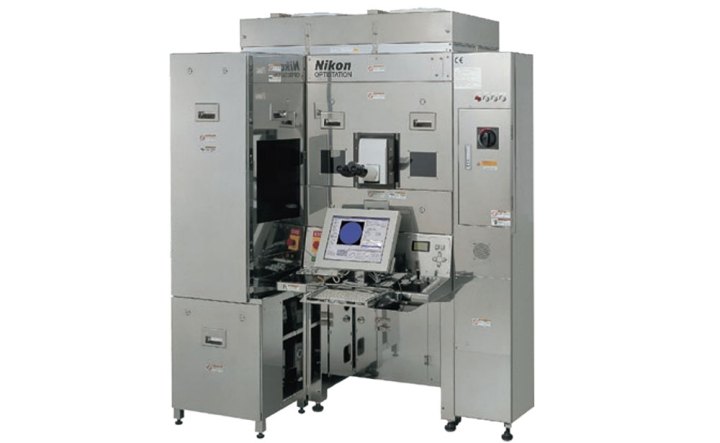
Nikon is making waves by announcing plans to lower the price of its lithography equipment by manufacturing several parts in-house to reduce overall costs. CEO Yasuhiro Ohmura, who took charge in April this year, told Nikkei Asia that Nikon is talking to several large chipmakers in the United States and Asia about supplying argon fluoride (ArF) tools, and some discussions are nearing purchase orders. The company also plans to launch a new ArF immersion platform—featuring a new lens and wafer stage—by 2028 while also building compatibility with ASML’s lithography tools. That’s crucial because, while price matters, problems arise when fab engineers try to align a layer on a Nikon tool back to a layer patterned with an ASML tool. It’s also important to note that while ASML enjoys a monopoly position in extreme ultraviolet (EUV) lithography systems, ArF immersion is a part of mature deep ultraviolet (DUV) technology. However, even 3-nm process nodes run many patterning steps on ArF immersion. In other words, this mature part of the DUV process remains important even for advanced chips. ASML directly competes with Japan’s Canon and Nikon in older DUV lithography equipment. However, ASML and Nikon are the only two firms that build ArF lithography equipment. Although their scanner technology roadmaps are completely different. The NSR-S625E ArF immersion scanner features a resolution of 38 nm, a numerical aperture of 1.35, and a 193-nm excimer laser. (Source: Nikon) The upside There’s broad consensus among industry watchers that ASML won’t lose sleep over Nikon’s DUV equipment sales. The real challenge will be if Nikon manages to build EUV machines, which are highly complex marvels of system engineering. Some industry observers call Nikon the next Intel, whose foundry bet was eventually rescued by a lack of fab capacity, while TSMC still dominates the chip contact manufacturing business. They reckon that Nikon’s move to lower prices of lithography solutions could help the fab equipment shortage caused by the supply backlog from ASML. Then there’s another dimension favoring Nikon: a single company having a monopoly on lithographic machines for semiconductor fabs is a red flag for the hypercompetitive chip industry. So, competition matters in the lithography market even if Nikon is years behind. And even when all three mega-fabs—Intel, Samsung, and TSMC—are shareholders of ASML. The downside For a start, as several market analysts note, price is largely irrelevant for the commercial specs of lithography machines. They point out that Nikon’s immersion scanners are already priced a double-digit percentage below ASML’s equivalent offering, and that Nikon’s market share is still declining. That’s one reason why Nikon intends to develop a completely new immersion scanner platform that’s technically competitive with an ASML scanner. Nikon’s upcoming scanner will incorporate a new projection lens to match ASML’s mask mirroring. The current masks in Nikon’s scanner can’t be shared with ASML. The upcoming scanner will also introduce a new wafer stage to enable correction of wafer stage hardware, allowing fabs to stop using multiple sets of scanners. However, as mentioned above, this new scanner is planned for launch by 2028, and a lot could change in the highly competitive lithography landscape during this period. Next comes the entrenchment factor. Fabs like TSMC have a long track record of working with ASML, and these fabs have acquired a deep technical expertise in integrating ASML components and systems into their manufacturing ecosystems. What if a lower-cost machine costs twice as much to integrate, or if it doesn’t achieve the required yield? Finally, as many in the industry point out, Nikon’s rise and fall mirrors what happened to the Japanese semiconductor industry at large over the past two decades or so. In retrospect, Japanese chipmakers and semiconductor equipment makers such as Canon and Nikon declined together. Can Nikon defy this downward trend? A quest for turnaround At a time when lithography is rapidly evolving, Nikon is making a bet on revival through close collaboration with key suppliers and research labs. But can it put a reverse to ASML’s “winner takes it all” story in the lithography world? Especially after losing the DUV race to ASML, now an undisputed leader with more than 8,000 semiconductor lithography systems installed worldwide? Nevertheless, Nikon needs a turnaround, and ASML’s advanced ArF immersion system, priced at around $82.5 million, smells like an opportunity. Add to this the fact that a few DUV machines usually accompany every EUV machine. Nikon’s strategic pivot to aggressively compete on price could also enable fabs to negotiate more effectively with ASML. Nikon is positioning itself as a second-source option for semiconductor fabs that don’t want to rely only on ASML. It will be interesting to see if Nikon can attract fabs with lower equipment costs and a second-source option.

Beyond the Factory Floor: XR Training for the Next Industrial Era
To say that Industry 4.0 will reshape manufacturing across Europe—and globally—would be an understatement. This Fourth Industrial Revolution is driving a more digital, data-driven future for manufacturers, with robotics and automation already transforming production lines, streamlining industrial processes, and creating new skills and opportunities for workforces. But as more and more robotics boost productivity and precision, workers and engineers must quickly get to grips with programming and operating these systems, often within complex and highly automated production environments—and this isn’t always easy. Workforce access to industrial robots can be limited due to cost, safety concerns, and a need to avoid disruption on the factory floor. But this is where initiatives such as the European Union Horizon project MASTER—Mixed Reality Ecosystem for Teaching Robotics in Manufacturing—are making an impact. Launched in January 2023 to support industrial robotics education and training, MASTER has developed an open, extended reality (XR) platform that exploits the latest virtual, augmented, and mixed reality technologies to provide immersive and interactive learning experiences for trainees. Organizations can build and run their own XR training and simulation environments in which several remote users can interact in real-time within the same scene, practicing tasks and experimenting with robotic systems in safe and controlled conditions. Master project coordinator Panagiotis Karagiannis For Panagiotis Karagiannis, MASTER project coordinator and project manager at the Laboratory for Manufacturing Systems and Automation (LMS), University of Patras, Greece, XR lies at the heart of Industry 4.0, and is set to, as he put it, “create a new paradigm” in training. “A lot of people can be afraid of new robotics—they can unexpectedly make quick movements and sudden sounds, which can be intimidating,” he said. “But working inside a digital environment with XR brings you closer to these systems without these problems—and we’ve created a training environment that feels like a game.” As the project draws to a close, the MASTER Open XR platform addresses the “fear of new technology” issue and more. Training factory workers through its immersive environment can also reduce a firm’s costs and circumvent the inevitable safety issues. “The platform is an affordable educational tool for factories,” Karagiannis highlighted. “You don’t need to develop the robots, you don’t need to set up the production line, you can create all of this virtually, which of course is cheaper.” “Also, in a manufacturing setting, numerous systems are operational, and safety can be very complex, bringing so many restrictions,” he added. “But by creating a digital environment, we avoid all of this.” Training for the masses MASTER’s Open XR training platform is based on an enterprise XR platform, VIROO, developed by Spanish VR tech firm Virtualware. Karagiannis and project colleagues have added three extra features to the platform to ease training: code-free robot programming, gaze-based interaction, and safe robotic environments, which mimic the factory floor by using virtual zones equipped with sensors to trigger a speed reduction or protective stop when a human enters the defined space. In addition to these features, EU-funded XR researchers have contributed new XR tools and educational content, via add-ons, to enhance the platform, which have all been tested via user studies. Examples include a voice-prompted tool for spawning, moving, and deleting objects such as robotic arms and forklifts, a photo-realistic digital twin of a cargo ship for maritime safety training, and a haptic glove so users can practice teleoperating a humanoid gripper in VR. User feedback, so far, has been positive with participants recommending applications to others, and reporting to be either “satisfied” or “very satisfied” with the platform’s ease of use. Content creators noted they would use the platform again for similar tasks, while trainees stated they enjoyed the graphics and interaction with 3D objects, and highlighted improvements in specific skills, particularly in understanding lecture content. Karagiannis also noted how the development and validation of these tools fostered significant collaboration, especially amongst SMEs. As a case in point, he highlighted a software development kit, “Dreamer,” that reconstructs 3D objects to be embedded in virtual scenes for training. Here, a self-supervised AI learning agent trained on streams of images rapidly extracts a 3D mesh representation of a physical object, so users can create content for populating simulated scenes. He then pointed out how, in a later sub-project, Xrplained, researchers used assets created in Dreamer to explore robot kinematics and better understand the complex principles behind robotic positioning, orientation, and motion. “We are proud of how we brought together different SMEs to develop, use, and customize different platform assets and exchange knowledge across different applications,” he said. But MASTER collaboration hasn’t just been about SMEs. Add-on developers have included researchers from larger firms, including Nokia Bell Labs. “All in all, the project has developed more than 30 assets—including 3D models, safety zones, as well as beautiful user interfaces and a virtual assistant—delivering a big impact,” Karagiannis commented. “We can really showcase to industry that through collaboration, we can create educational scenarios that deliver good results and provide a supportive environment for the training operators and engineers.” A user tests an advanced virtual reality headset and motion-tracking controllers, which feature exposed LED tracking rings for precise spatial positioning. (Source: European Union Horizon) Next moves As well as being based on Viroo’s enterprise-ready platform, MASTER Open XR platform is compatible with Open XR and ROS, an open-source framework for robot software development. This interoperability enables integration into existing industrial environments, allowing the platform to be more easily adopted by organizations across Europe and beyond, where it can be further developed and scaled for myriad manufacturing applications. Looking ahead, the focus will shift from platform development to ecosystem expansion and real-world deployment. Karagiannis would like to see project groups within organizations developing even more virtual assets and scenarios that will grow the platform even further. “We could see the platform move beyond education—additional XR assets could also be used for, say, technical support and maintenance,” he said. Further into the future, Karagiannis firmly believes that AI could be integrated across the platform to generate yet more XR assets and add-ons. “XR is one of Industry 4.0’s core technologies because it deeply involves humans in industrial processes and, as we reach Industry 5.0, with its even more human-centric approach, we will see this to an even greater extent,” he said. “There is so much potential for our platform here.”