TSMC Defends Transistor Scaling Amid Huawei’s ‘Her’s Law’ Proposal
AMSTERDAM, The Netherlands — At TSMC’s European Symposium, Kevin Zhang, senior VP and deputy co-chief operating officer at market-leading foundry TSMC, responded to questions from reporters about Huawei’s proposal to stop measuring industry progress on transistor density.
Huawei proposed Her’s Law, analogous to Moore’s Law, based on Tao scaling, a method of measuring industry progress in terms of overall speedup rather than purely on transistor density. Huawei does not have access to EUV machines necessary to shrink transistor geometries beyond 7-nm process nodes.
Asked about Huawei’s Tao scaling theory, Zhang said that while he had not looked into it in detail, Tao scaling appears to be a matter of 3D integration, which can bring different functions closer together to reduce delays between chips.
“I think that the concept [of 3D integration] has been around in this industry for long enough,” he said. “This is something, obviously, we’re going to continue work with our customers to drive forward. That’s how I look at it.”
Fundamentally, the transistor is still critical, Zhang said.
“Remember, all the computation is done at the transistor level, so don’t forget how important the transistor is,” he added. “If you look at the overall R&D effort, transistor development continues to consume the most R&D effort to drive the next generations of technology. Transistor technology takes tremendous effort.”
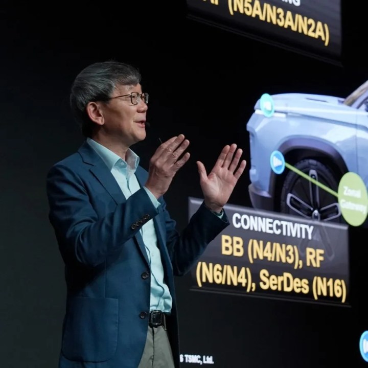
Kevin Zhang presents at TSMC’s European Symposium in Amsterdam (Source: TSMC)
Transistor technology scaling on its own can give you 30% better energy efficiency when moving from N2 to A14. “That’s the number, it’s absolutely significant,” Zhang said.
To illustrate, Zhang pointed towards a growing movement in the data center world to deliver 800 V directly to racks, which means replacing entire power delivery systems. This is a considerable task which improves energy efficiency by only low-single-digit percentage points, Zhang said. By comparison, shrinking transistor geometries between N2 and A14 process nodes would reduce power by 30%.
Transistor geometry shrinking as practiced by TSMC is the industry’s key vector for increasing transistor density today. TSMC has access to EUV technology and its roadmap is based on shrinking the geometry of its transistors.
In the ISCAS keynote, Huawei claimed their 3D stacking method increases density per square millimeter despite not adding more transistors to any individual die. Zhang was generous when asked about the Chinese hyperscaler’s new definition of “density.”
“Density, in my view, is no longer measured in two dimensions,” he said. “It’s measured by space. The vertical dimension also comes in when you talk about overall space.”
Die stacking is certainly an innovative way to increase computation density, Zhang said.
“Stacking gives you another dimension to continue to increase the computation per cubic centimeter,” he said. “When you build a data center, you really think about the three-dimensional space, that’s how important it is.”
TSMC is looking at technologies like CFETs (complementary field-effect transistors) for future transistors. Zhang said CFETs are attractive precisely because they are stacked in three dimensions. CFETs comprise a p-type FET stacked on top of an n-type FET, within the same die, effectively building two transistors in the space previously occupied by one.
TSMC’s European venture, ESMC in Dresden, is on track, Zhang said. The foundry leader broke ground almost two years ago for the fabs, which will focus on automotive and industrial products. Tools should be installed in the new fabs by 2027, but the overall ramp schedule will be based on market conditions and customer needs, the company said.